Method for forming metal wires in semiconductor device

A semiconductor and metal wire technology, applied in the field of metal wires forming semiconductor devices, can solve problems such as uneven buried characteristics

Inactive Publication Date: 2005-06-01
SK HYNIX INC
View PDF0 Cites 0 Cited by
  • Summary
  • Abstract
  • Description
  • Claims
  • Application Information

AI Technical Summary

Problems solved by technology

[0005] However, as shown in Figures 1 and 2, the CECVD method has non-uniform burying characteristics in burying the contact holes of ultra-fine structures

Method used


Image

  • Method for forming metal wires in semiconductor device
  • Method for forming metal wires in semiconductor device
  • Method for forming metal wires in semiconductor device

Examples


Embodiment Construction

[0018] Reference will now be made in detail to the preferred embodiments of the invention, examples of which are illustrated in the accompanying drawings.

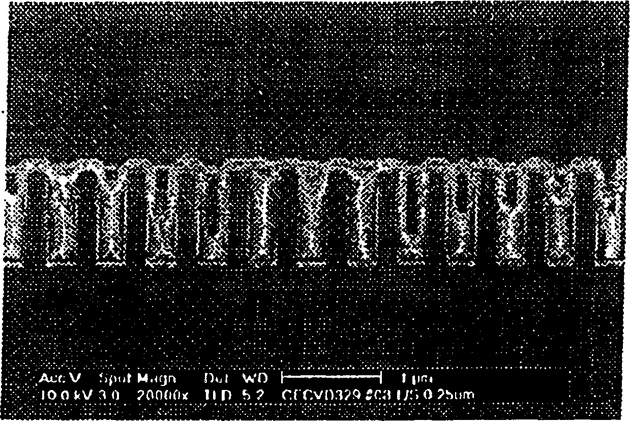
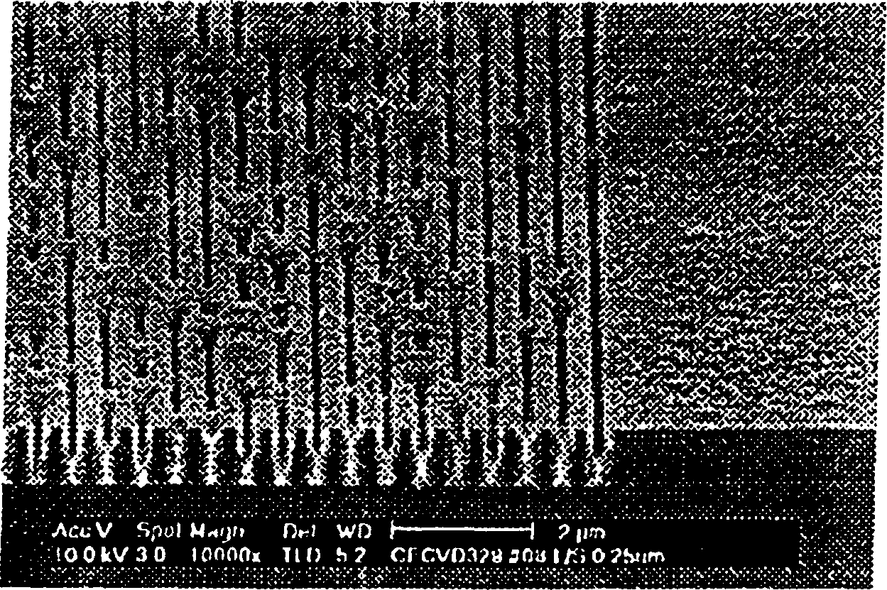
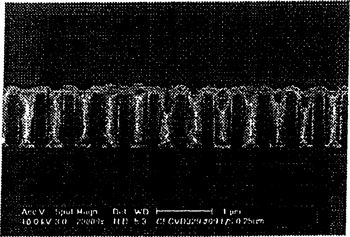
[0019] 3a to 3e are sectional views of a semiconductor device for explaining a method of forming a metal line of a semiconductor device according to the present invention.

[0020] Referring to FIG. 3a, an interlayer insulating layer 12 is formed on a semiconductor substrate 11 having a predetermined structure by using an insulating film of low dielectric constant. A pattern is formed in the interlayer insulating layer 12 by a single damascene method or a dual damascene method to form a damascene pattern. After the rinsing process is performed, on the intermediate insulating layer 12 in which the mosaic pattern is formed, the diffusion barrier layer 13 is formed. When the low-level structures are tungsten (W) and aluminum (Al) structures, the rinsing process is performed with RF plasma. And when the low-order structure i...


PUM


Abstract

The present invention discloses a method for forming a metal line of a semiconductor device, in which a Cu thin film is deposited on a diffusion diaphragm layer after chemical enhancer and plasma treatment, thereby improving the burying characteristics of a contact hole with an ultrafine structure . The method comprises the following steps: forming an intermediate insulating film layer on a semiconductor substrate with a predetermined low-level structure; forming a mosaic pattern in the interlayer insulating film layer; forming a diffusion barrier layer on the entire structure with the mosaic pattern; chemical enhancer treatment on the diffusion membrane layer to form a chemical enhancer film on the diffusion membrane layer; plasma treatment; Cu thin film formation on the entire structure to bury the mosaic pattern; and polishing treatment to expose the intermediate The upper surface of the insulating film layer, causing the Cu thin film to remain in the mosaic model.

Description

technical field [0001] The present invention relates to a method for forming a metal wire of a semiconductor device, and more particularly to such a method for forming a metal wire of a semiconductor device, wherein after a chemical enhancer and a plasma treatment, a diffusion barrier film (diffusion barrier film) ) to deposit a layer of Cu thin film, thereby improving the buried characteristics of the contact hole (contact hole) with ultra-fine structure. Background technique [0002] With the high-performance trend of advanced semiconductor devices, the size of contact holes has decreased while their aspect ratios have increased rapidly. In this regard, excellent step coverage is required, and contact holes need to be buried. [0003] Such advanced semiconductor devices mainly use Cu thin films as metal wire materials. A method of forming a Cu thin film will be briefly described below. An intermediate insulating film layer is formed on a semiconductor substrate with a p...

Claims


Application Information

Patent Timeline
Patent Type & Authority Patents(China)
IPC IPC(8): C23C16/18H01L21/28H01L21/285H01L21/768
CPCH01L21/28556H01L21/76807H01L21/76814H01L21/76843H01L21/76862H01L21/76876H01L21/76877H01L21/28
Inventor 表成奎
Owner SK HYNIX INC
Why Eureka
Try Eureka