
Design method for improving PCB bow

A design method and bowing technology, applied in printed circuits, electrical components, printed circuit manufacturing, etc., can solve problems such as PCB bowing, and achieve the effects of reducing internal stress, uniform copper distribution, and consistent heating speed

Pending Publication Date: 2022-08-05
SHENZHEN SUNTAK MULTILAYER PCB
View PDF5 Cites 0 Cited by
  • Summary
  • Abstract
  • Description
  • Claims
  • Application Information

AI Technical Summary

Problems solved by technology

[0006] In view of the above-mentioned existing technical defects, the present invention provides a design method for improving PCB bow, which solves the problem of PCB bow without affecting production efficiency and production cost

Method used


Image

  • Design method for improving PCB bow
  • Design method for improving PCB bow

Examples


Embodiment

[0029] A design method for improving PCB bowing shown in this embodiment includes the following steps in turn:

[0030] a. The copper clad core board is cut out according to the size of the panel of 520mm×620mm, with the long side as the warp direction and the short side as the weft direction.

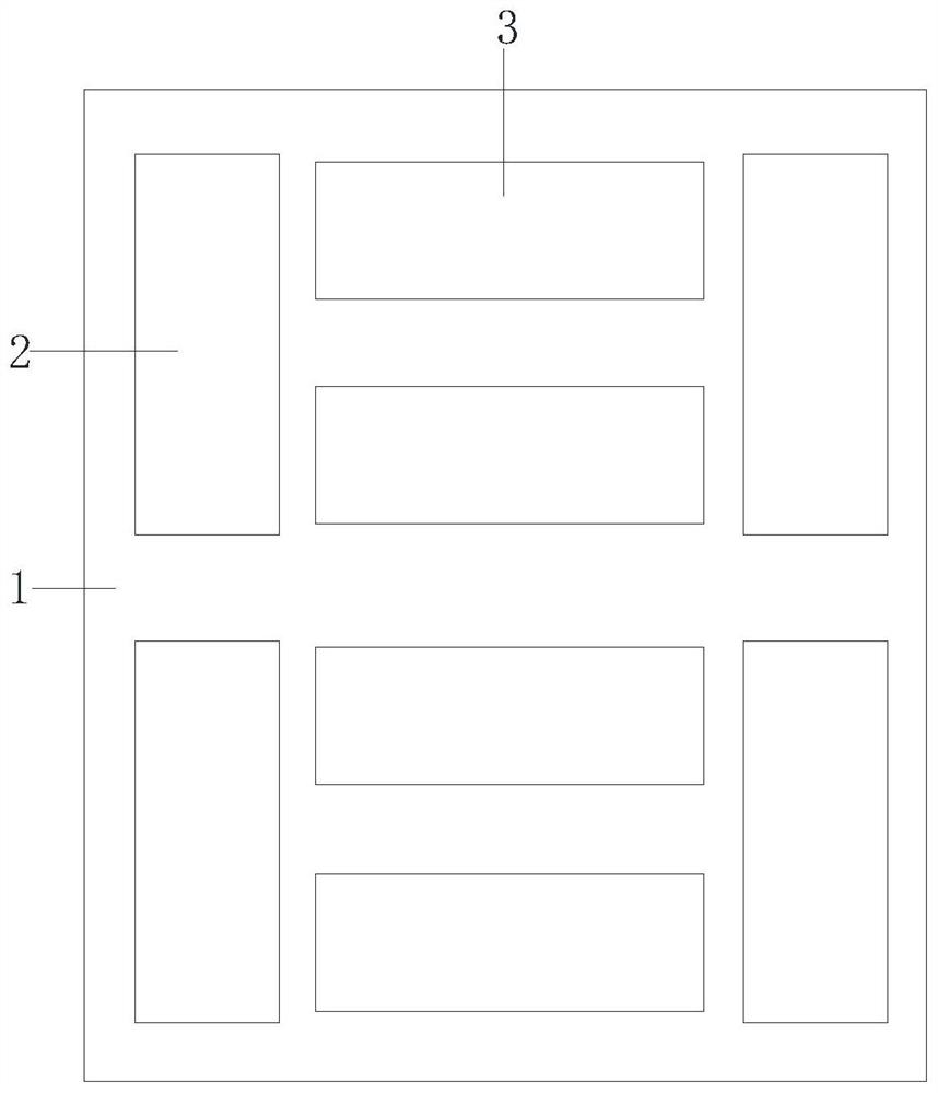
[0031] b. If figure 1 As shown in the figure, the copper clad core board is typeset to design a number of circuit board units (ie SET boards) on the copper clad core board according to the typesetting requirements, and each circuit board unit includes at least one unit board (ie PCS) ; Wherein, at least two columns of first circuit board units 2 whose length direction is parallel to the meridian direction of the copper clad core board are arranged on the copper clad core board 1, and at least one column of length is set between the first circuit board units 2 of two adjacent columns. The second circuit board unit 3 whose direction is parallel to the latitudinal direction of the CCL, t...


PUM


Abstract

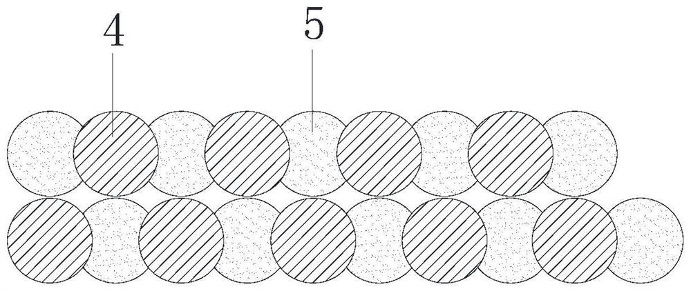
The invention discloses a design method for improving PCB bow, which comprises the following steps: providing a square copper-clad core plate, and taking the long side of the square copper-clad core plate as the warp direction and the short side as the weft direction; typesetting the copper-clad core plate; wherein at least two columns of first circuit board units of which the length direction is parallel to the warp direction of the copper-clad core board are arranged on the copper-clad core board, and at least one column of second circuit board units of which the length direction is parallel to the weft direction of the copper-clad core board is arranged between two adjacent columns of first circuit board units; when an inner layer circuit is manufactured on the copper-clad core board, copper surfaces outside the first circuit board unit and the second circuit board unit are etched into a plurality of PADs which are arranged at intervals, and the PADs on the upper surface and the lower surface of the copper-clad core board are arranged in a staggered mode. According to the method, the layout distribution design and the PAD design of the non-unit board area are changed, so that the problem of PCB bending is solved under the condition that the production efficiency and the production cost are not influenced.

Description

technical field [0001] The invention relates to the technical field of manufacturing printed circuit boards, in particular to a design method for improving PCB bowing. Background technique [0002] PCB bowing refers to the deformation of the printed circuit board similar to the shape of a curved ball. PCB bowing can lead to quality problems such as lead angle deviation and virtual soldering when assembling components. [0003] The main reason for PCB bowing is: in the laminated structure of PCB design, the thickness of the core board is asymmetrical up and down, and the thin core board after lamination is insufficiently supported to cause warpage. [0004] Excessive bowing of the PCB leads to deviations in the external dimensions and the position of the positioning holes. In the subsequent mechanical assembly process, the components cannot be inserted into the PCB holes and pads, resulting in serious quality problems. The conventional lamination structure core board and the...

Claims


Application Information

Patent Timeline
Patent Type & Authority Applications(China)
IPC IPC(8): H05K3/36H05K3/02
CPCH05K3/36H05K3/02
Inventor 张盼盼邹金龙宋建远樊锡超
Owner SHENZHEN SUNTAK MULTILAYER PCB
Learn More