
Graphic design method for reducing dry film breakage of fine circuit board

A graphic design and fine circuit technology, applied in the direction of conductive pattern formation, etc., can solve the problems of circuit open circuit, gap, dry film broken resistance plating, etc., to achieve the effect of ensuring completeness, reducing dry film broken, and avoiding film clamping

Pending Publication Date: 2022-08-05
GUANGZHOU MEADVILLE ELECTRONICS
View PDF0 Cites 0 Cited by
  • Summary
  • Abstract
  • Description
  • Claims
  • Application Information

AI Technical Summary

Problems solved by technology

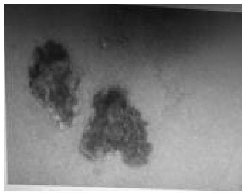
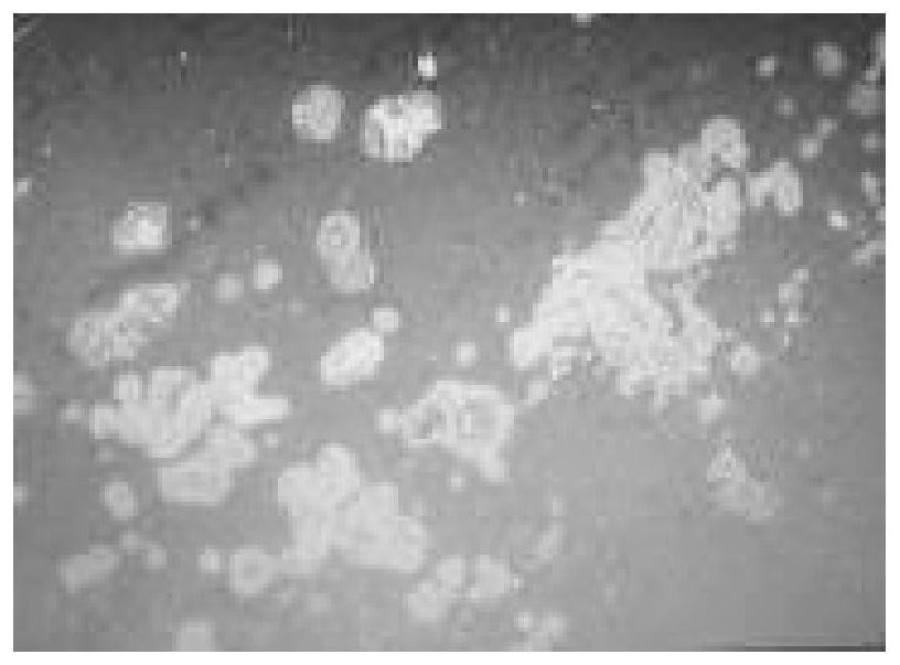
At this stage, in the circuit board industry, the line width and line spacing level of the circuit can be 30 / 30μm, and the circuit is even finer. The modified semi-additive process (mSAP) has been introduced. Due to the special nature of the process, tiny debris or dry film debris can cause plating resistance, resulting in open circuits or gaps

Method used


Image

  • Graphic design method for reducing dry film breakage of fine circuit board
  • Graphic design method for reducing dry film breakage of fine circuit board
  • Graphic design method for reducing dry film breakage of fine circuit board

Examples


Embodiment Construction

[0027] The present invention will be further described below with reference to the specific embodiments. It should be noted that, on the premise of no conflict, the embodiments or technical features described below can be arbitrarily combined to form new embodiments.

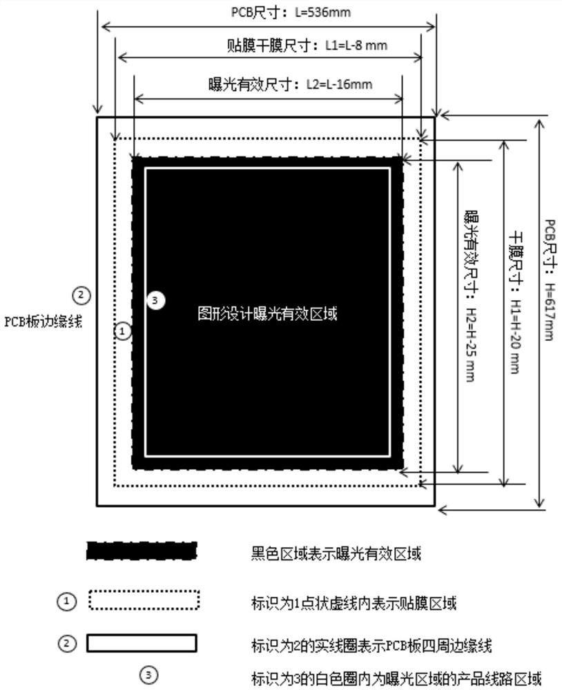
[0028] Please see attached Figures 4 to 7 The present invention provides a graphic design method for reducing dry film breakage of fine circuit boards. Specifically, on the PCB board after the dry film is attached, the dry film needs to have a certain distance from the edge of the circuit board to ensure that there is a certain distance around the dry film. Sufficient space is reserved for auxiliary alignment holes, test mold positions, test coupon positions, equipment fixture clip positions and board edge flow grooves, from Figure 4 It can be seen from the schematic diagram that after the development of the circuit board provided by the present invention, there is no dry film residue on the clip position on t...


PUM


Abstract

A graphic design method for reducing dry film breakage of a fine circuit board relates to the technical field of fine circuit board manufacturing, and a dry film on a PCB (printed circuit board) after the dry film is pasted needs to be a certain distance away from the edge of the circuit board so as to ensure that enough space is reserved around the dry film to reserve various mold positions. And dry film breakage caused by the fact that the clamp is clamped on the plate edge dry film is avoided. According to the graphic design method for reducing the dry film fragments of the fine circuit board, generation of the dry film fragments can be avoided and controlled from the source, and the quality influence of circuit open circuit or notch caused by the fact that the dry film fragments adhere to the board surface to hinder electroplating is avoided.

Description

technical field [0001] The invention belongs to the technical field of fine circuit board manufacturing, and in particular relates to a graphic design method for reducing dry film breakage of a fine circuit board. Background technique [0002] With the continuous upgrading of circuit boards, the circuit boards gradually move towards the process of small, light, thin and thin, so the requirements for the line width and line spacing of the lines are getting higher and higher, and the line width is getting thinner and thinner. At this stage, the circuit board industry can achieve the line width and line spacing level of 30 / 30μm, and even the lines are more refined. The improved semi-additive process (mSAP) has been introduced. The lines produced by the mSAP process are often very fine, but due to the process Due to the special nature of the process, often tiny debris or dry film fragments can cause plating resistance, resulting in open circuits or gaps. How to reduce or avoid ...

Claims


Application Information

Patent Timeline
IPC IPC(8): H05K3/10
CPCH05K3/108H05K2203/0548
Inventor 王宏业姚晓建区健唐
Owner GUANGZHOU MEADVILLE ELECTRONICS
Learn More