


Quick Research
Generate reliable direction feasibility study reports for your R&D in just a few steps.

Technical Q&A
Discover and master advanced knowledge NOW. Basics, ideas, possibilities, all at once.

Find Solutions
As an expert in R&D theories, this can generate solutions to your technical problems instantly.

Evaluate Feasibility
Analyze your overall solution with one click, know your potential R&D risks in advance.

Monitor Landscape
Get weekly tech updates, stay abreast of the latest tech innovations and key insights.
Optical response semiconductor switch with short circuit load protection
A load protection, semiconductor technology, applied in the field of light-responsive semiconductor switches, can solve problems such as unsatisfactory
- Summary
- Abstract
- Description
- Claims
- Application Information
AI Technical Summary
Problems solved by technology
Method used
Image

Examples
no. 1 example
[0044] First embodiment (Fig. 1)
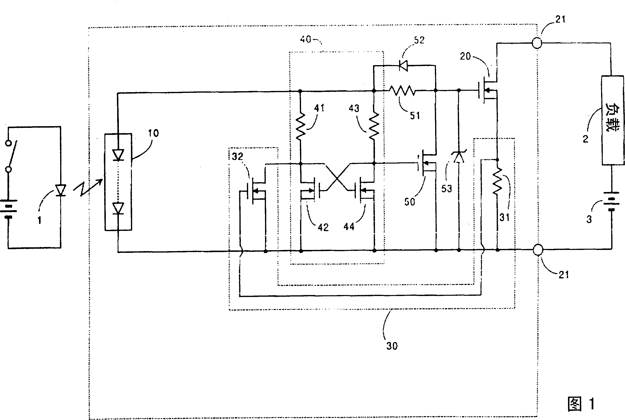
[0045] Referring to FIG. 1, it shows a photoresponsive semiconductor switch according to a first embodiment of the present invention. The switch is used in combination with the light emitting diode 1 to form a photorelay for connecting and disconnecting the load 2 with the power source 3 . The switch comprises photoelectric elements 10 in the form of an array of photodiodes, which generate electricity when light is absorbed from light emitting diodes 1 . This electrical energy gives an operating voltage that decreases as the current to the photodiode array 10 increases. The operating voltage is applied to activate an output switching transistor 20 in the form of an n-channel enhancement metal oxide field effect transistor (MOSFET) whose gate-source is connected across the photodiode array 10 . The drain and source of the output MOSFET 20 are respectively connected to an output terminal 21 suitable for connection to a load circuit consisting...
no. 2 example
[0052] Second embodiment (Fig. 4)
[0053] Referring to FIG. 4, it shows a photoresponsive semiconductor switch according to a second embodiment of the present invention. The switch of this embodiment is designed for a load circuit powered by an AC source 3A to a load 2, and is identical to the first embodiment except for the use of an additional output MOSFET 22, and an additional current sensing resistor 33 and an additional sensor MOSFET 34 in the overload sensor 30A. Example is the same. Like elements are designated by like reference numerals with an "A" suffix. The additional output MOSFET 22 is connected in series with the output MOSFET 20A between the output terminals 21A, the sources of the MOSFETs 20A and 22 are connected to each other, and the gates of the MOSFETs 20A and 22 are connected together to receive the operating voltage of the photodiode array 10A. An additional resistor 33 is connected in series with terminal 31A between output terminals 21A, providing a...
no. 3 example
[0057] The third embodiment (Fig. 7)
[0058] Referring to FIG. 7, there is shown a third embodiment of an optically responsive semiconductor switch of the present invention which is identical to the first embodiment except that a bypass MOSFET 35 is included in the overload sensor 30D. Like elements are designated by like reference numerals with a "D" suffix. The source-drain of the bypass MOSFET 35 is connected in series with the current response resistor 31D, connected to both ends of the drain-source of the output MOSFET 20D, and its gate is connected to the gate of the output MOSFET 20D to jointly receive the operating voltage from the photodiode array 10D . Bypass MOSFET 35 and resistor 31D form a high resistance path across output MOSFET 20D so that only a small portion flows through resistor 31D for overload detection, while most of the load current flows through output MOSFET 20D. When overload sensor 30D detects an overload, latch circuit 40D is responsive to keepi...
PUM
 Abstract
Description
Claims
Application Information
 - R&D Engineer
- R&D Manager
- IP Professional
- Industry Leading Data Capabilities
- Powerful AI technology
- Patent DNA Extraction
Browse by: Latest US Patents, China's latest patents, Technical Efficacy Thesaurus, Application Domain, Technology Topic, Popular Technical Reports.
© 2024 PatSnap. All rights reserved.Legal|Privacy policy|Modern Slavery Act Transparency Statement|Sitemap|About US| Contact US: help@patsnap.com