
Light-emitting backboard and manufacturing method thereof

A technology of a light-emitting backplane and a manufacturing method, which is applied in optics, nonlinear optics, instruments, etc., can solve the problems of light-emitting occlusion of LED lamps, uneven thickness of white oil layer, light reflection effect of LED lamps, etc., so as to improve the thickness Uniformity, reducing white oil smearing, and improving the effect of light output

Active Publication Date: 2022-07-22
TCL CHINA STAR OPTOELECTRONICS TECH CO LTD
View PDF10 Cites 0 Cited by
  • Summary
  • Abstract
  • Description
  • Claims
  • Application Information

AI Technical Summary

Problems solved by technology

[0003] In Mini LED backlight modules, a white oil layer is often coated on the substrate to reflect light. However, in the existing white oil layer manufacturing process, if you want to achieve high-precision white oil, make the white oil layer very close to the LED lamp. On the one hand, it is easy to block the light of the LED lamp, and on the other hand, it is easy to cause the tail to be too long, resulting in uneven thickness of the white oil layer. If the white oil layer is too far away from the LED lamp, it is difficult to control the light around the LED lamp. It plays a reflective role, resulting in the phenomenon of black under the lamp, and it is difficult to avoid the influence of the white oil layer on the light output effect of the Mini LED backlight module under the premise of ensuring the high precision of the white oil layer

Method used


Image

  • Light-emitting backboard and manufacturing method thereof
  • Light-emitting backboard and manufacturing method thereof
  • Light-emitting backboard and manufacturing method thereof

Examples


Embodiment Construction

[0038] The technical solutions in the embodiments of the present invention will be clearly and completely described below with reference to the accompanying drawings in the embodiments of the present invention. Obviously, the described embodiments are only some, but not all, embodiments of the present invention. Based on the embodiments of the present invention, all other embodiments obtained by those skilled in the art without creative efforts shall fall within the protection scope of the present invention.

[0039] The following disclosure provides many different embodiments or examples for implementing different structures of the present invention. In order to simplify the disclosure of the present invention, the components and arrangements of specific examples are described below. Of course, they are only examples and are not intended to limit the invention. Furthermore, the present disclosure may repeat reference numerals and / or reference letters in different instances ...


PUM

PropertyMeasurementUnit
lengthaaaaaaaaaa
angleaaaaaaaaaa

Abstract

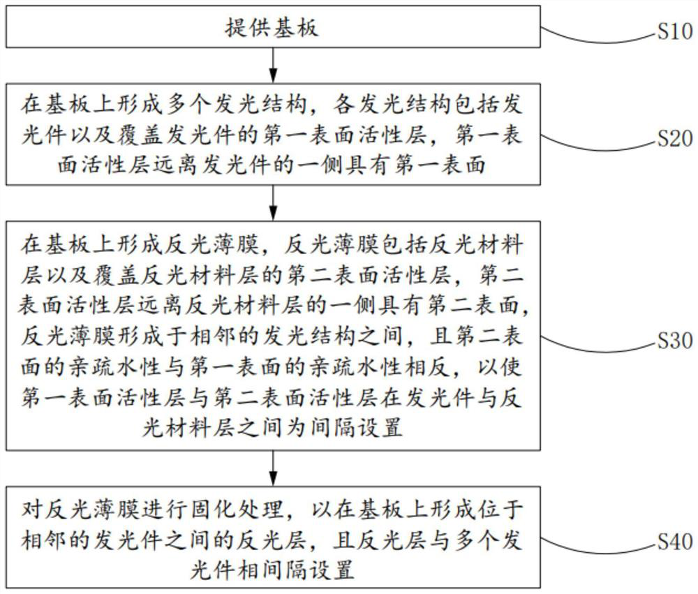
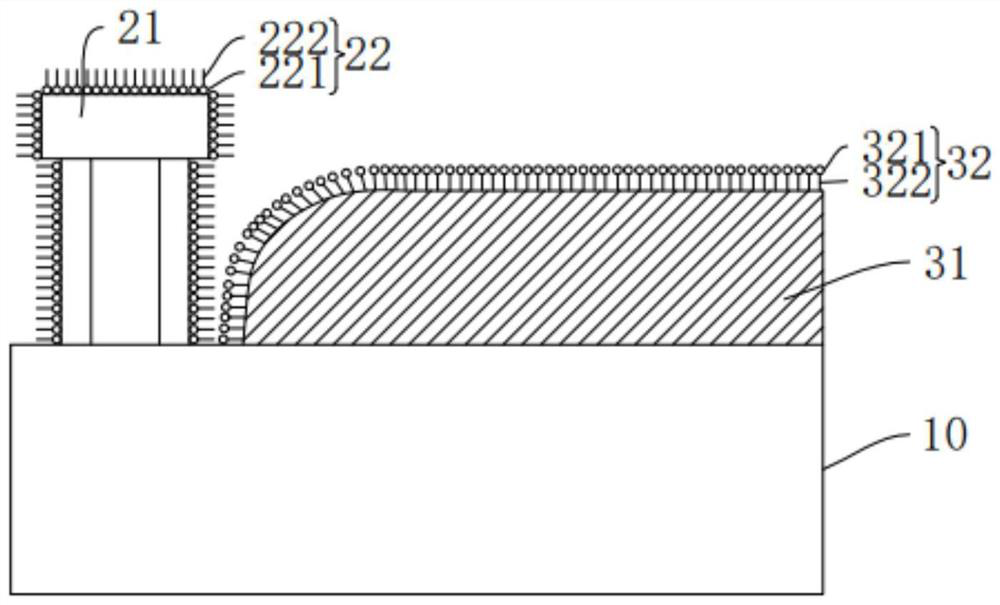
The invention discloses a light-emitting backboard and a manufacturing method thereof. The method comprises the following steps: providing a substrate; a plurality of light-emitting structures are formed on the substrate, each light-emitting structure comprises a light-emitting part and a first surface active layer covering the light-emitting part, and the side, away from the light-emitting part, of the first surface active layer is provided with a first surface; a reflective film is formed on the substrate and comprises a reflective material layer and a second surface active layer covering the reflective material layer, the side, away from the reflective material layer, of the second surface active layer is provided with a second surface, the reflective film is formed between the adjacent light-emitting structures, and the hydrophilic-hydrophobic property of the second surface is opposite to the hydrophilic-hydrophobic property of the first surface; the first surface active layer and the second surface active layer are separated between the light-emitting part and the light-reflecting material layer; and curing the reflective film to form a reflective layer located between the adjacent light-emitting parts on the substrate, the reflective layer being spaced from the plurality of light-emitting parts. According to the invention, the coverage precision and thickness uniformity of the reflective layer can be improved.

Description

technical field [0001] The present invention relates to the field of display technology, and in particular, to a light-emitting backplane and a manufacturing method thereof. Background technique [0002] The LCD (Liquid Crystal Display, liquid crystal display) screen with Mini LED backlight module is increasingly becoming one of the hot spots of future display technology, compared with the current LCD and OLED (Organic Light-Emitting Diode, organic light-emitting diode) display devices , has the advantages of fast response, high color gamut, high PPI, and low energy consumption. Among them, Mini LED is also known as sub-millimeter light-emitting diode. Its size is usually 80 microns to 200 microns. It is a new generation of LED technology. It undertakes the characteristics of high efficiency, high reliability, high brightness and fast response time of small-pitch LEDs. And LEDs with smaller pitches consume less power and cost less. [0003] In Mini LED backlight modules, a...

Claims


Application Information

Patent Timeline
Patent Type & Authority Applications(China)
IPC IPC(8): G02F1/13357
CPCG02F1/133603G02F1/133605
Inventor 邓红照
Owner TCL CHINA STAR OPTOELECTRONICS TECH CO LTD
Learn More