
IP unit, logic control chip and three-dimensional stacked chip

A logic control and chip technology, applied in electrical components, instruments, electrical digital data processing, etc., can solve problems such as too long signal transmission lines, signal attenuation, etc., and achieve the effect of solving the problem of signal attenuation

Pending Publication Date: 2022-07-05
XI AN UNIIC SEMICON CO LTD
View PDF0 Cites 0 Cited by
  • Summary
  • Abstract
  • Description
  • Claims
  • Application Information

AI Technical Summary

Problems solved by technology

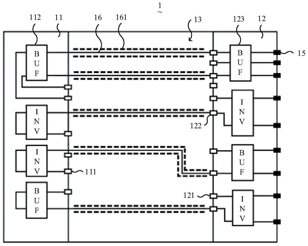
[0003] The application at least provides an IP unit, a logic control chip and a three-dimensional stacked chip, which are used to solve the problem of signal attenuation caused by too long signal transmission lines

Method used


Image

  • IP unit, logic control chip and three-dimensional stacked chip
  • IP unit, logic control chip and three-dimensional stacked chip
  • IP unit, logic control chip and three-dimensional stacked chip

Examples


Embodiment Construction

[0029] In order for those skilled in the art to better understand the technical solutions of the present application, the IP unit, logic control chip and three-dimensional stacked chip provided by the present application will be described in further detail below with reference to the accompanying drawings and specific embodiments. It should be understood that the described embodiments are only a part of the embodiments of the present application, but not all of the embodiments. Based on the embodiments in the present application, all other embodiments obtained by those of ordinary skill in the art without creative efforts shall fall within the protection scope of the present application.

[0030] The terms "first", "second", etc. in this application are used to distinguish different objects, rather than to describe a specific order. Furthermore, the terms "comprising" and "having" and any variations thereof are intended to cover non-exclusive inclusion. For example, a process...


PUM


Abstract

The invention discloses an IP unit, a logic control chip and a three-dimensional stacked chip, the IP unit comprises a first device module, a second device module and a control module, and the control module is located between the first device module and the second device module and is connected with the first device module and the second device module; the IP unit further comprises a signal output end, the first device module and the second device module are used for conducting signal enhancement processing on the data interaction signals output by the control module, and the signal output end is used for outputting the processed data interaction signals to an external control unit. The first device module and the second device module are arranged on the two sides of the control module, and signal enhancement processing is performed on the data interaction signal output by the control module through the first device module and the second device module, so that the problem of signal attenuation caused by an overlong signal transmission line is solved.

Description

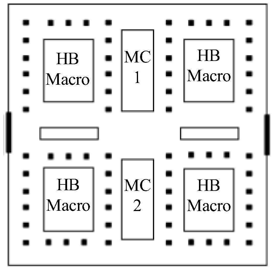
technical field [0001] The present application relates to the field of logic control chips, and in particular, to an IP unit and a logic control chip. Background technique [0002] In the 3D integrated circuit design, the logic control chip and the DRAM chip perform data interaction through the macro cell (HB Macro). In the process of data exchange, there are a large number of signal traces set across macrocells, resulting in too long lines, signal integrity is affected when signals are connected across macrocells, and timing violations are easily caused. SUMMARY OF THE INVENTION [0003] The present application provides at least an IP unit, a logic control chip and a three-dimensional stacked chip, which are used to solve the problem of signal attenuation caused by too long signal transmission lines. [0004] A first aspect of the present application provides an IP unit. The IP unit includes a first device module, a second device module, and a control module. The control...

Claims


Application Information

Patent Timeline
IPC IPC(8): G06F30/394G06F30/396H01L25/18H01L27/02G06F115/08
CPCG06F30/394G06F30/396H01L27/0207H01L25/18G06F2115/08
Inventor 林文博
Owner XI AN UNIIC SEMICON CO LTD
Learn More