Thin transfer conductive structure
A conductive structure and transfer technology, applied in the direction of connection, circuit, contact parts, etc., can solve the problems of large hidden dangers and cumbersome branch wiring, and achieve the effect of eliminating hidden dangers and not easy to fall off by itself.
- Summary
- Abstract
- Description
- Claims
- Application Information
AI Technical Summary
Problems solved by technology
Method used
Image
Examples
specific Embodiment 1
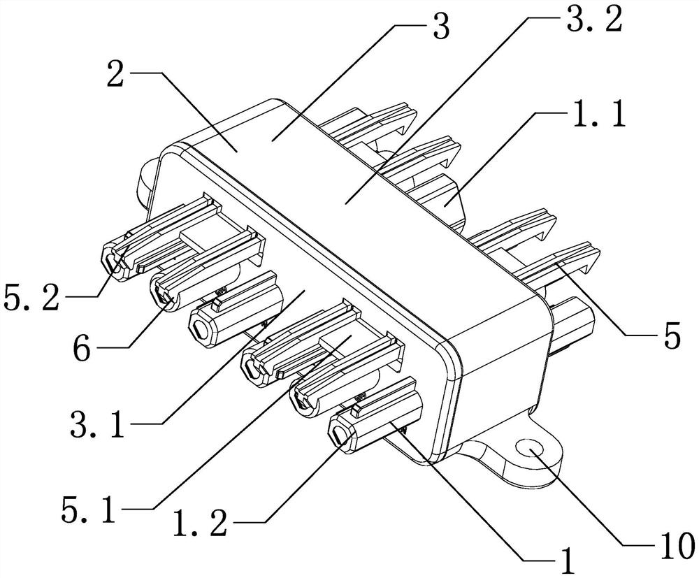
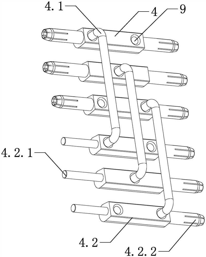
[0031] like figure 1 or figure 2As shown, a thin transfer conductive structure includes a transfer structure 1 and a conductive structure 4, the transfer structure 1 is connected by a conductive structure 4, and the conductive structure 4 includes a number of metal pins 4.2 and a number of metal pins for connecting In the connector 4.1 of 4.2, there are several connection holes 9 on the metal pin 4.2, and the connector 4.1 is adapted to the connection hole 9; the metal pin 4.2 includes the first metal pin 4.2.1 for connecting the incoming line and the The second metal pin 4.2.2; the conductive structure 4 is provided with a thin adapter shell 3 adapted to the conductive structure 4, and the adapter structure 1 is fixed on the thin adapter shell 3; There are a number of clips 5 for clamping with the plug; the clip 5 includes a limit block 5.1 and a number of bumps 5.2, and the bumps 5.2 arranged on the same clip 5 are connected through the limit block 5.1. The length of the ...
specific Embodiment 2
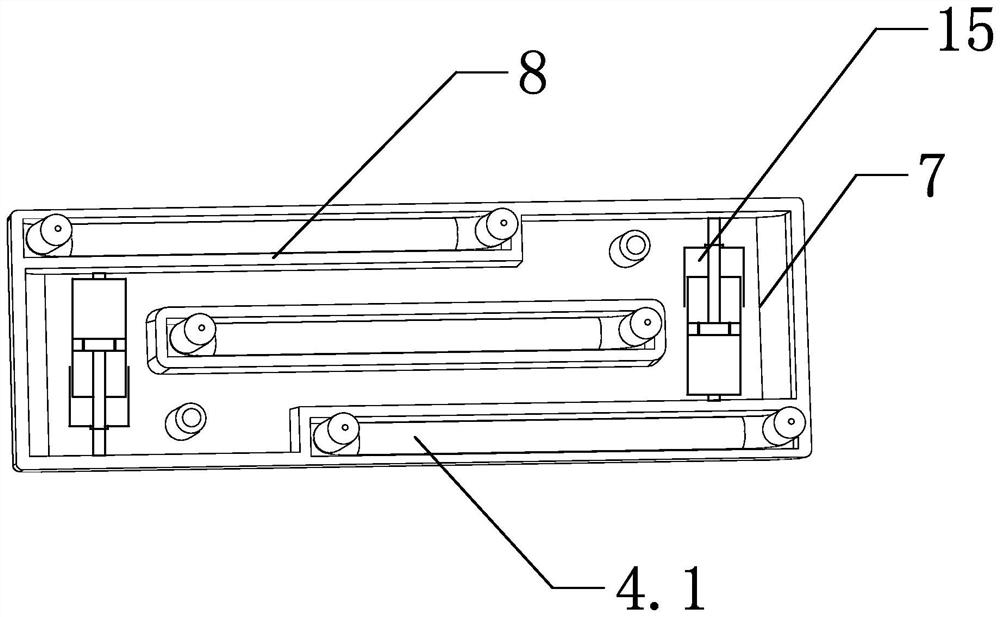
[0033] like image 3 As shown, on the basis of Embodiment 1, an intermediate reinforcing plate 7 is arranged between the conductive structure 4 and the thin adapter shell 3, and the intermediate strengthening plate 7 is clamped with the thin adapter shell 3; the bottom of the intermediate strengthening plate 7 is provided with A number of grooves 8 are matched with the connecting piece 4.1, and a shock absorber 15 for vibration damping is embedded in the middle reinforcing plate 7.
[0034] In the above technical solution, the middle reinforcing plate is arranged between the conductive structure 4 and the thin adapter shell 3 and is clamped with the thin adapter shell 3, so that the connecting piece does not directly contact the thin adapter shell 3, preventing the The leakage of electricity can make the adapter compact in structure, strengthen the force effect of the adapter, and increase the impact resistance and extrusion resistance of the adapter; there are several grooves...
specific Embodiment 3
[0035] like Figure 4 or Figure 5 As shown, on the basis of Embodiment 2, the thin adapter shell 3 includes a front cover 3.1 and a rear cover 3.2, the front cover 3.1 is integrally formed, the rear cover 3.2 is integrally formed, and the front cover 3.1 and the rear cover 3.2 are ultrasonically welded; 3.1 is provided with a positioning column 13, and a positioning hole 14 for matching with the positioning column 13 is provided on the rear cover 3.2.
[0036] In the above technical solution, the front cover 3.1 and the rear cover 3.2 are respectively integrally formed, which is convenient for processing and has a beautiful appearance. The front cover 3.1 and the rear cover 3.2 are welded by ultrasonic waves. Ultrasonic welding uses high-frequency vibration waves to transmit to the surfaces of the two objects to be welded. , In the case of pressure, the surfaces of the two objects are rubbed against each other to form fusion between the molecular layers, the welding material...
PUM
| Property | Measurement | Unit |
|---|---|---|
| thickness | aaaaa | aaaaa |
Abstract
Description
Claims
Application Information
 - R&D Engineer
- R&D Manager
- IP Professional
- Industry Leading Data Capabilities
- Powerful AI technology
- Patent DNA Extraction
Browse by: Latest US Patents, China's latest patents, Technical Efficacy Thesaurus, Application Domain, Technology Topic, Popular Technical Reports.
© 2024 PatSnap. All rights reserved.Legal|Privacy policy|Modern Slavery Act Transparency Statement|Sitemap|About US| Contact US: help@patsnap.com


