LED chip and preparation method thereof

A technology of LED chips and omnidirectional mirrors, applied in semiconductor devices, electrical components, circuits, etc., can solve problems such as junction temperature rise, heat generation, and reduction of LED chip electro-optical conversion efficiency, so as to reduce junction temperature and reduce light emission. , Improve the effect of electro-optical conversion

Pending Publication Date: 2022-05-24
YANGZHOU CHANGELIGHT
View PDF0 Cites 0 Cited by
  • Summary
  • Abstract
  • Description
  • Claims
  • Application Information

AI Technical Summary

Problems solved by technology

However, although it has been possible to design the openings on the dielectric layer to be staggered from the N electrodes, when the current passes through the epitaxial layer, because the epitaxial layer is conductive, part of the current will still spread laterally to the active layer below the N electrode to emit light, and this part of the light will be emitted. The N electrode blocks or absorbs, thereby generating heat and increasing the junction temperature, which reduces the electro-optical conversion efficiency of the LED chip

Method used


Image

  • LED chip and preparation method thereof
  • LED chip and preparation method thereof
  • LED chip and preparation method thereof

Examples


Embodiment Construction

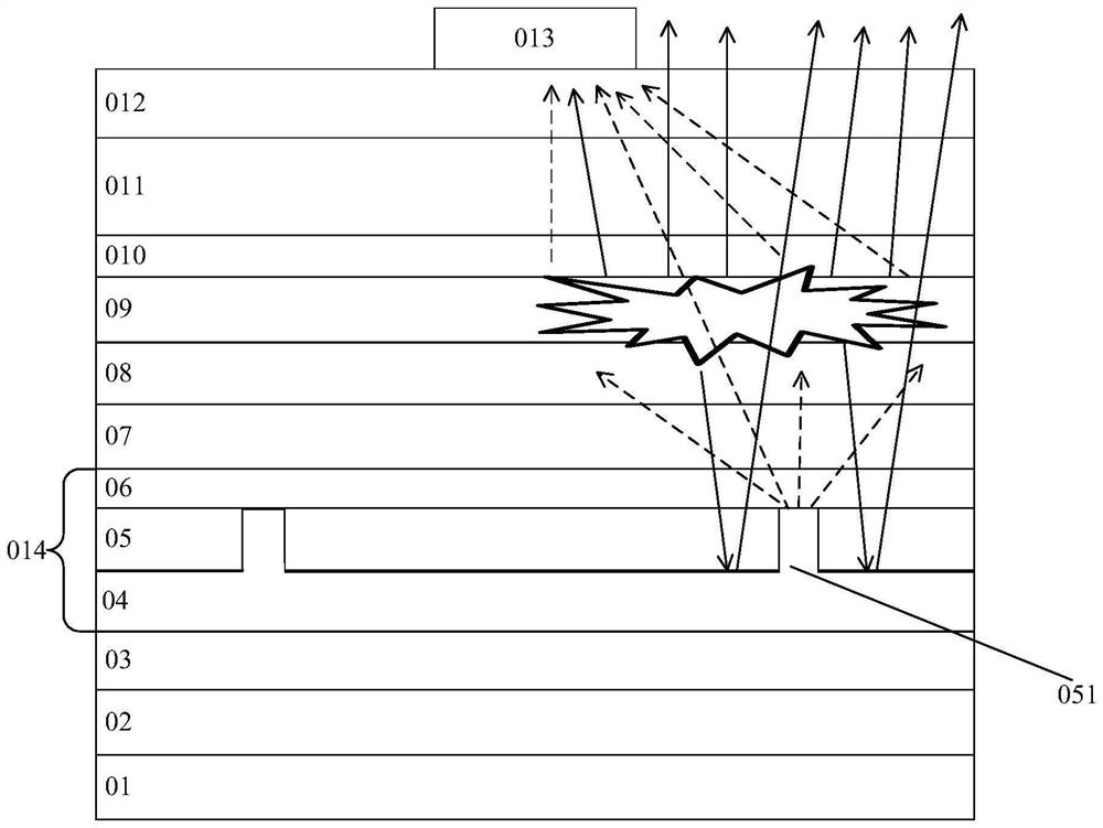
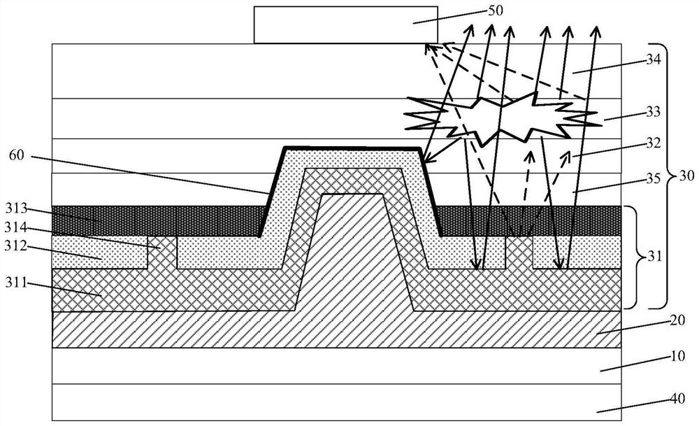
[0047] The technical solutions in the embodiments of the present application will be clearly and completely described below with reference to the drawings in the embodiments of the present application. Obviously, the described embodiments are only a part of the embodiments of the present application, but not all of the embodiments. Based on the embodiments in the present application, all other embodiments obtained by those of ordinary skill in the art without creative efforts shall fall within the protection scope of the present application.

[0048] Many specific details are set forth in the following description to facilitate a full understanding of the present application, but the present application can also be implemented in other ways different from those described herein, and those skilled in the art can do so without departing from the connotation of the present application. Similar promotion, therefore, the present application is not limited by the specific embodiments...


PUM

PropertyMeasurementUnit
thicknessaaaaaaaaaa

Abstract

The invention discloses an LED chip and a preparation method thereof, and the method comprises the steps: carrying out the at least partial etching of a lamination layer which is composed of at least an ohmic contact layer and a part of a first type semiconductor layer in a second electrode shielding region, and forming a groove, therefore, current flowing into the active layer of the second electrode shielding area from the ohmic contact layer of the second electrode shielding area and a part of the first type semiconductor layer can be reduced at least, that is, the current transversely expanded into the active layer of the second electrode shielding area is reduced, the light emission of the active layer of the second electrode shielding area is reduced, heat production is reduced, and the service life of the device is prolonged. The purposes of reducing the junction temperature and improving the electro-optical conversion efficiency of the LED chip are achieved, meanwhile, more current can be expanded to the active layer which is not shielded by the second electrode, and the electro-optical conversion efficiency of the LED chip is further improved.

Description

technical field [0001] The present application relates to the technical field of light-emitting diodes, and in particular, to an LED chip and a preparation method thereof. Background technique [0002] With the development of light-emitting diode (Light-Emitting Diode, LED) chip technology, the internal quantum efficiency of LEDs has reached a very high level, but the light extraction efficiency is still relatively low, which needs to be improved urgently. At present, high-brightness light-emitting LED chips usually use an omni-directional reflector (ODR), so as to improve the reflection efficiency of the reflector, thereby improving the light extraction efficiency. [0003] The omnidirectional mirror usually includes a semiconductor layer, a dielectric layer and a metal mirror layer, which are arranged on the P side of the LED chip. In order to ensure that the semiconductor layer and the metal mirror layer form ohmic contact, it is necessary to open holes in the dielectric ...

Claims


Application Information

Patent Timeline
Patent Type & Authority Applications(China)
IPC IPC(8): H01L33/10H01L33/00H01L33/14H01L33/38H01L33/46
CPCH01L33/10H01L33/145H01L33/382H01L33/46H01L33/005
Inventor 伏兵李晓静赵鹏马英杰蔡和勋
Owner YANGZHOU CHANGELIGHT
Why Eureka
Try Eureka