RF MEMS device and preparation method thereof

A device and substrate technology, applied in the field of microelectronics, can solve problems affecting the performance of radio frequency systems and the performance of MEMS devices

Pending Publication Date: 2022-05-24
TSINGHUA UNIV
View PDF0 Cites 0 Cited by
  • Summary
  • Abstract
  • Description
  • Claims
  • Application Information

AI Technical Summary

Problems solved by technology

Due to the large size of PCB board-level interconnection, additional parasitic loss will be introduced; SiP can reduce the loss caused by interconnection to a certain extent, but the welding, bonding and other process steps and the short-distance mutual interference between chips are still Will have an impact on the performance of MEMS devices
Especially in the millimeter wave frequency band, the parasitic phenomenon caused by the interconnection will be more serious, and even affect the performance of the radio frequency system

Method used


Image

  • RF MEMS device and preparation method thereof
  • RF MEMS device and preparation method thereof
  • RF MEMS device and preparation method thereof

Examples


Embodiment Construction

[0037] The following describes in detail the embodiments of the present invention, examples of which are illustrated in the accompanying drawings, wherein the same or similar reference numerals refer to the same or similar elements or elements having the same or similar functions throughout. The embodiments described below with reference to the accompanying drawings are exemplary, and are intended to explain the present invention and should not be construed as limiting the present invention.

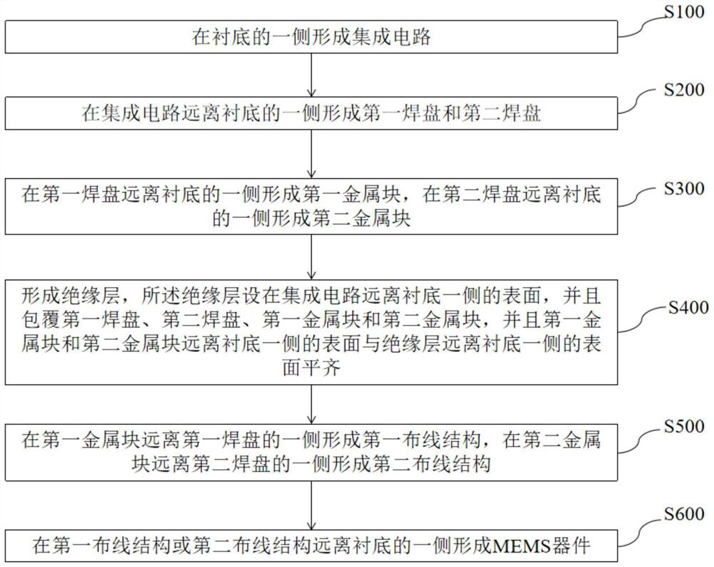
[0038] In order to improve the above technical problems, the present invention provides an RF MEMS device, refer to figure 1 , the RF MEMS device includes a substrate 1, a first pad 21, a second pad 22, a first metal block 43, a second metal block 44, an insulating layer 5, a first wiring structure 61, a second wiring structure 62 and MEMS device 7.

[0039] According to an embodiment of the present invention, one side of the substrate 1 is provided with an integrated circuit (not shown...


PUM

PropertyMeasurementUnit
Heightaaaaaaaaaa
Thicknessaaaaaaaaaa

Abstract

The invention provides an RF MEMS device and a preparation method thereof, and the RF MEMS device comprises a substrate, one side of which is provided with an integrated circuit; the first bonding pad and the second bonding pad are arranged on the integrated circuit; the first metal block is arranged on the first bonding pad, and the second metal block is arranged on the second bonding pad; the insulating layer wraps the first bonding pad, the second bonding pad, the first metal block and the second metal block, and the surfaces of the sides, away from the substrate, of the first metal block and the second metal block are not wrapped by the insulating layer; the first wiring structure is connected with the first metal block, and the second wiring structure is connected with the second metal block; at least one of the first wiring structure and the second wiring structure is connected with the MEMS device. Therefore, interconnection between the integrated circuit and the MEMS device can be realized, and loss caused by interconnection can be effectively reduced.

Description

technical field [0001] The invention belongs to the technical field of microelectronics, and particularly relates to an RF MEMS device and a preparation method thereof. Background technique [0002] MEMS devices are regarded as candidates for future RF wireless systems such as 5G, radar, and satellite communications due to their low insertion loss, high isolation, and high linearity. However, the interconnection between MEMS devices and other integrated circuits (such as drive circuits, microwave integrated circuits) is an important factor affecting their radio frequency performance. At present, in order to realize the interconnection between MEMS devices and other integrated circuits, PCB board-level interconnection and SiP (System-in-Package) are mainly used. Due to the large size of PCB board-level interconnection, additional parasitic loss will be introduced; SiP can reduce the loss caused by interconnection to a certain extent, but the process steps such as welding and...

Claims


Application Information

Patent Timeline
IPC IPC(8): B81B7/00B81B7/02B81C1/00
CPCB81B7/007B81B7/02B81C1/00246B81C1/00349B81B2201/01
Inventor 刘泽文张玉龙
Owner TSINGHUA UNIV
Why Eureka
Try Eureka