
Boost circuit

A technology of boosting circuit and boosting capacitor is applied in the direction of conversion equipment without intermediate conversion to AC, which can solve the problems of small conduction loss and large conduction loss, so as to achieve small conduction loss, reduce power loss, The effect of improving circuit efficiency

Pending Publication Date: 2022-05-17
JOULWATT TECH INC LTD
View PDF0 Cites 0 Cited by
  • Summary
  • Abstract
  • Description
  • Claims
  • Application Information

AI Technical Summary

Problems solved by technology

[0016] The purpose of the present invention is to provide a boost circuit and boost method with less conduction loss, which solves the problem of large conduction loss in the prior art

Method used


Image

  • Boost circuit
  • Boost circuit
  • Boost circuit

Examples


Embodiment Construction

[0043] Preferred embodiments of the present invention will be described in detail below with reference to the accompanying drawings, but the present invention is not limited to these embodiments. The present invention covers any alternatives, modifications, equivalent methods and schemes made within the spirit and scope of the present invention.

[0044] In order to provide the public with a thorough understanding of the present invention, specific details are set forth in the following preferred embodiments of the present invention, but those skilled in the art can fully understand the present invention without the description of these details.

[0045] In the following paragraphs the invention is described more specifically by way of example with reference to the accompanying drawings. It should be noted that all the drawings are in a relatively simplified form and use inaccurate scales to facilitate and clearly assist the purpose of illustrating the embodiments of the prese...


PUM


Abstract

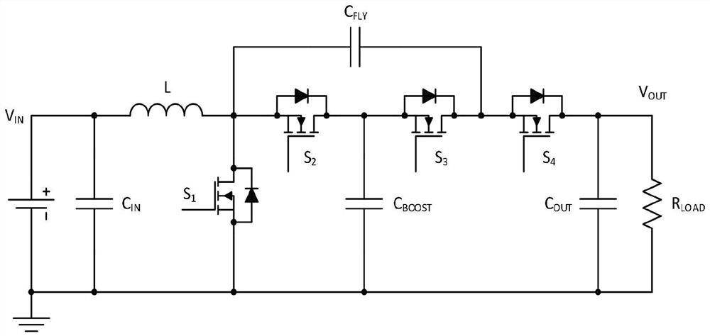
The boost circuit is based on an input inductor, a flying capacitor and a boost capacitor, and the first end of the input inductor is connected with an input power supply; the flying capacitor is connected with the second end of the input inductor; the boost capacitor is connected with the flying capacitor and the input inductor through a switching tube; voltage boosting of an input power supply is realized by controlling charging and discharging of the input inductor, the flying capacitor and the boosting capacitor. The boost circuit is small in conduction loss and high in boost efficiency.

Description

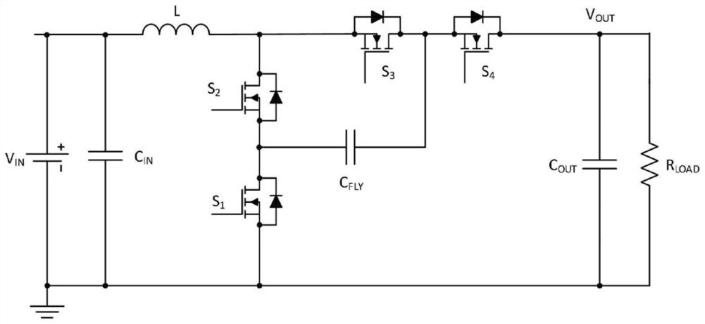
technical field [0001] The invention relates to the field of power electronics, in particular to a voltage boosting circuit. Background technique [0002] The boost circuit has a simple topology and simple control, and is widely used on the DC / DC side of photovoltaic inverters. For low-voltage systems, the two-level boost circuit can meet the withstand voltage requirements. However, for higher input voltages, due to the Most of the general-purpose power tubes are low-voltage devices, and the price of high-voltage devices is several times that of low-voltage devices. It is difficult for two-level boost circuits to meet the withstand voltage requirements. [0003] figure 1 shows an existing three-level boost circuit, the input voltage is V IN , the output voltage is V OUT , in the first time period t1, the switches S1 and S2 are turned on, and the inductor L is charged; in the second time period t2, the switches S1 and S3 are turned on, and the inductor L discharges to the ...

Claims


Application Information

Patent Timeline
IPC IPC(8): H02M3/04H02M3/07
CPCH02M3/04H02M3/07
Inventor 何勇吉
Owner JOULWATT TECH INC LTD
Learn More