Bionic neuron memristor and preparation method thereof
A technology of neurons and memristors, applied in the field of bionic neurons, can solve the problems that robots do not have an emotional system and their responses are not as sensitive as living organisms
- Summary
- Abstract
- Description
- Claims
- Application Information
AI Technical Summary
Problems solved by technology
Method used
Image
Examples
Embodiment 1
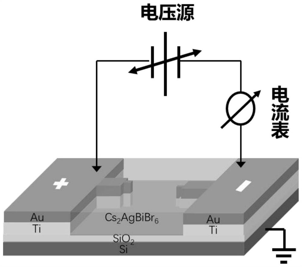
[0040] This embodiment provides a bionic neuron memristor, such as figure 1 As shown, including a substrate, parallel electrodes and a dielectric layer; the parallel electrodes and the dielectric layer are all arranged on the substrate;
[0041] The parallel counter electrodes include a positive electrode layer and a negative electrode layer, and the medium layer is arranged between the positive electrode layer and the negative electrode layer;
[0042] The dielectric layer adopts a semiconductor material containing low activation energy ions in the crystal lattice;
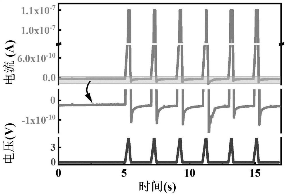
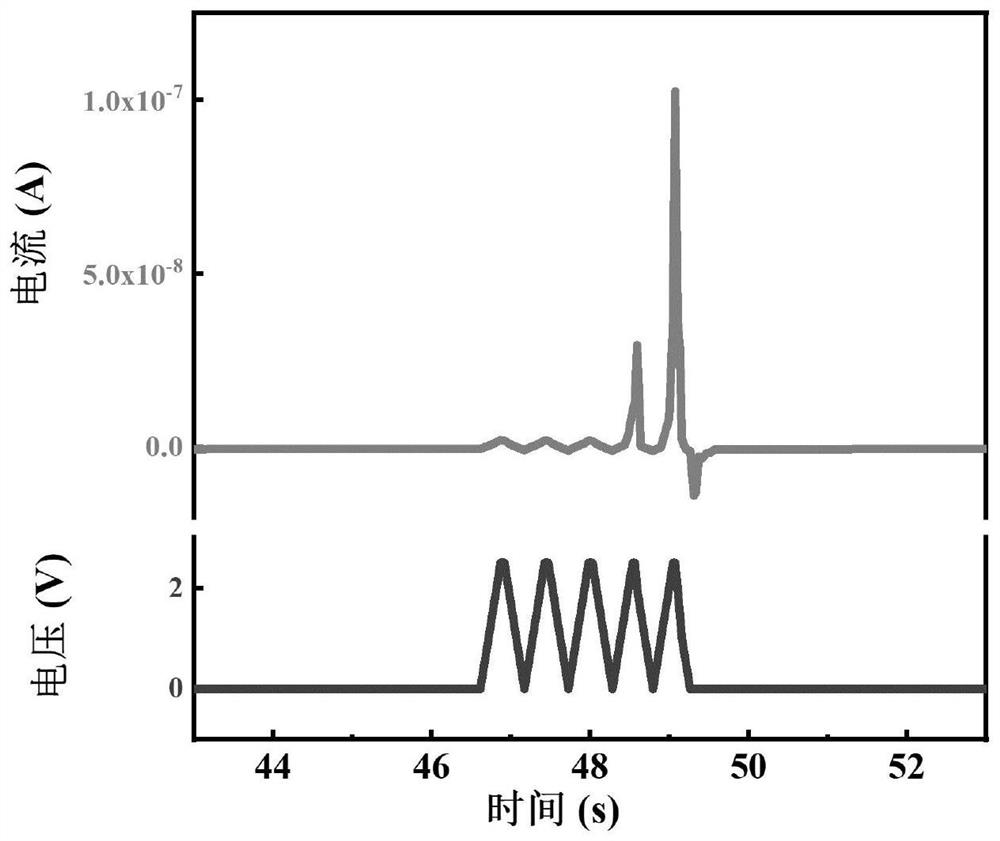
[0043] There are two kinds of low activation energy ions in the lattice in the dielectric layer. Driven by the electric field, the two low activation energy ions are regulated by the electric field and move to the positive and negative poles respectively, which is used to simulate the sodium and potassium ions inside and outside the neuron membrane when stimulated. The process of membrane potential changes resul...
Embodiment 2
[0066] This embodiment provides a method for preparing a bionic neuron memristor, such as Figure 8 As shown, the method includes the steps of:
[0067] S1: Prepare a precursor solution, dissolve CsBr, BiBr3, and AgBr in dimethyl sulfoxide at a ratio of 2:1:1, heat and stir at 75°C for 4 hours, and prepare 10ml of a 0.4mol / mL transparent solution;
[0068] S2: Put the silicon wafer into acetone and alcohol respectively, ultrasonically clean it in deionized water for 10 hours, take it out and dry it with nitrogen;
[0069] S3: Spin-coat the cleaned silicon wafer with photoresist, expose the silicon wafer to ultraviolet light for 3s, and then put it into the developer solution for development for 45s;
[0070] S4: Put the developed silicon wafer into the electron beam evaporation deposition system for deposition, the pressure is below 1x10⁻⁵Pa, first deposit 5nm Ti electrode, and then deposit 80nm Au electrode;
[0071] S5: Place the deposited sheet in the glue-removing soluti...
PUM
| Property | Measurement | Unit |
|---|---|---|
| Thickness | aaaaa | aaaaa |
| Thickness | aaaaa | aaaaa |
| Thickness | aaaaa | aaaaa |
Abstract
Description
Claims
Application Information
 - R&D
- Intellectual Property
- Life Sciences
- Materials
- Tech Scout
- Unparalleled Data Quality
- Higher Quality Content
- 60% Fewer Hallucinations
Browse by: Latest US Patents, China's latest patents, Technical Efficacy Thesaurus, Application Domain, Technology Topic, Popular Technical Reports.
© 2025 PatSnap. All rights reserved.Legal|Privacy policy|Modern Slavery Act Transparency Statement|Sitemap|About US| Contact US: help@patsnap.com


