Cleaning tool and cleaning method for semiconductor wafer

A technology for semiconductors and wafers, applied in the field of cleaning tooling for semiconductor wafers, achieves the effects of good cleaning effect, prevention of collapse, and simple and convenient operation

Active Publication Date: 2022-04-22
BEIJING CHENJING ELECTRONICS
View PDF6 Cites 1 Cited by
  • Summary
  • Abstract
  • Description
  • Claims
  • Application Information

AI Technical Summary

Problems solved by technology

[0004] The present invention provides a cleaning tool and cleaning method for semiconductor wafers, which are used to solve or improve at least one technical problem existing in the prior art, so as to improve cleaning operation efficiency, ensure cleaning effect, and prevent semiconductor wafers from collapsing during cleaning. , broken or laminated

Method used


Image

  • Cleaning tool and cleaning method for semiconductor wafer
  • Cleaning tool and cleaning method for semiconductor wafer
  • Cleaning tool and cleaning method for semiconductor wafer

Examples


Embodiment Construction

[0028] In order to make the purpose, technical solutions and advantages of the present invention clearer, the technical solutions in the present invention will be clearly and completely described below in conjunction with the accompanying drawings in the present invention. Obviously, the described embodiments are part of the embodiments of the present invention , but not all examples. Based on the embodiments of the present invention, all other embodiments obtained by persons of ordinary skill in the art without creative efforts fall within the protection scope of the present invention.

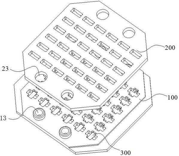
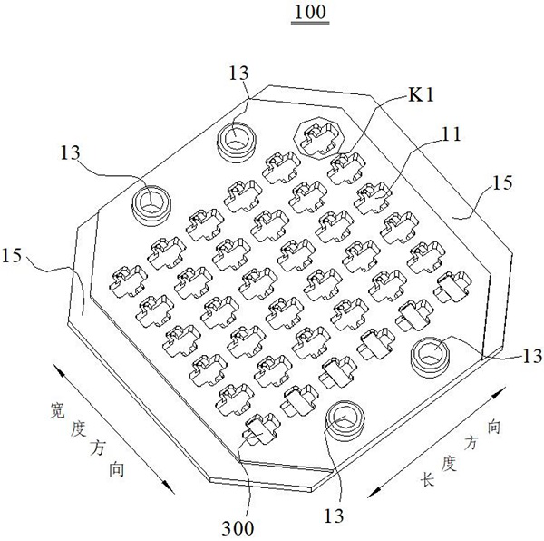
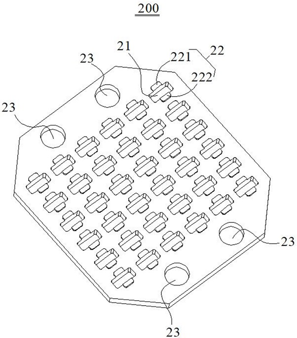
[0029] Combine below Figure 1-Figure 9 A semiconductor wafer cleaning tool and cleaning method of the present invention are described.

[0030] Such as Figure 1 to Figure 8 As shown, the present embodiment provides a semiconductor wafer cleaning tool, including: a first splint 100 and a second splint 200; The first surface of the second splint 200 is opposite to each other. Wherein, whe...


PUM

PropertyMeasurementUnit
thicknessaaaaaaaaaa

Abstract

The invention provides a cleaning tool and a cleaning method for a semiconductor wafer. The cleaning tool for the semiconductor wafer comprises a first clamping plate and a second clamping plate, a plurality of first through holes are formed in the first clamping plate, and a sinking groove is formed in one side of each first through hole; the sinking groove is formed in the first surface of the first clamping plate, the opening end of the sinking groove is formed in the hole wall of the first through hole, and the sinking groove and the first through hole form a communicating structure; a plurality of second through holes are formed in the second clamping plate, a protrusion is arranged on one side of each second through hole, and the protrusions are arranged on the first surface of the second clamping plate; the multiple first through holes are opposite to the multiple second through holes in a one-to-one mode, one end of the protrusion is located in the sinking groove, and a containing space is defined in the communicating structure based on the end face of the protrusion and the groove bottom of the sinking groove. According to the semiconductor wafer cleaning device, the semiconductor wafers can be conveniently separated and stored, the semiconductor wafers are prevented from being stacked in the cleaning process, the semiconductor wafers can be fully cleaned, the semiconductor wafers are prevented from being broken, damaged or stacked in the cleaning process, and therefore the good cleaning effect is achieved.

Description

technical field [0001] The invention relates to the technical field of semiconductors, in particular to a semiconductor wafer cleaning tool and cleaning method. Background technique [0002] At present, when cleaning small-sized semiconductor wafers, a large number of semiconductor wafers are first put into a mesh cleaning basket, and then cleaned by an automatic cleaning machine. After the cleaning process is completed, the semiconductor wafers are introduced into the crucible for alcohol dehydration , and finally, the semiconductor wafer is dried on the electric heating plate. [0003] In actual operation, the above-mentioned cleaning method mainly has various defects or deficiencies, which are mainly reflected in the following two aspects: first, semiconductor wafers are easy to be stacked in the cleaning basket, and the overlapping parts between semiconductor wafers have insufficient cleaning and cleaning effect The poor problem caused most of the semiconductor wafers t...

Claims


Application Information

Patent Timeline
Patent Type & Authority Applications(China)
IPC IPC(8): B08B11/02H01L21/02H01L21/67
CPCB08B11/02H01L21/6704H01L21/67051H01L21/02041
Inventor 郭春霞李智魏金鑫兰宇张健王纪东王颖何远
Owner BEIJING CHENJING ELECTRONICS
Why Eureka
Try Eureka