GaN-based device isolation method

A device isolation and metal film technology, which is applied in semiconductor devices, semiconductor/solid-state device manufacturing, electrical components, etc., can solve the problems of device reliability decline, low leakage, and high resistance, and achieve low defect density, low leakage, and high resistance. Effect

Pending Publication Date: 2022-04-01
ZHEJIANG UNIV HANGZHOU GLOBAL SCI & TECH INNOVATION CENT
View PDF0 Cites 0 Cited by
  • Summary
  • Abstract
  • Description
  • Claims
  • Application Information

AI Technical Summary

Problems solved by technology

[0006] In order to solve the defects caused by the traditional device isolation process that will form leakage channels, thereby affecting the reliability of the device, the present invention provides a GaN-based device isolation method. The device isolation region is prepared by the method of the present invention, and the defect density in the isolation region is small. High resistance and low leakage, which solves the problem of device reliability degradation caused by defects caused by traditional device isolation methods

Method used


Image

  • GaN-based device isolation method

Examples


Embodiment

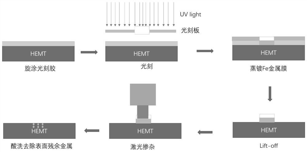
[0032] see figure 1 , the present invention provides a method for GaN-based device isolation, comprising the following steps:

[0033] Step 1): Expose the area where device isolation needs to be done on the surface of the sample by photolithography;

[0034] Step 2): Evaporate a layer of Fe metal film on the surface of the sample, the purity of the Fe source used is 99.999%, and the electron beam pressure is 10 -6 Torr, evaporation rate 0.5-3nm / min, Fe metal film thickness 1-20nm;

[0035] Step 3): The Lift-off process removes the excess Fe metal film, leaving the area that needs to be isolated to cover the Fe metal film;

[0036] Step 4): The Fe metal film is irradiated with laser pulses, the wavelength of the laser used in the experiment is 1030nm, the pulse width is 0.13ps, the average power is 30-70mW, and the laser repetition frequency is 2000Hz;

[0037] The high-energy laser pulse melts the sample locally, the Fe element diffuses into the sample, and Fe is incorporat...


PUM

PropertyMeasurementUnit
thicknessaaaaaaaaaa
thicknessaaaaaaaaaa
wavelengthaaaaaaaaaa

Abstract

The invention discloses a method for isolating a GaN-based device, which comprises the following steps of: evaporating a Fe film on a region, which needs to be subjected to device isolation, on the surface of a GaN HEMT structure, heating the Fe film to cover the region by adopting pulse laser, reasonably controlling laser pulse energy, accelerating Fe to diffuse into a sample and recrystallizing the sample, thereby merging Fe into a sample crystal lattice. Fe impurities are deep-energy-level impurities in the GaN-based material, and a high-resistance state can be formed by doping Fe in a region needing to be isolated, so that the aim of device isolation is fulfilled. According to the method, a sample is recrystallized through high-energy laser pulses, and Fe impurities are introduced in the recrystallization process, so that the defect density of an isolation region can be reduced.

Description

technical field [0001] The invention belongs to the technical field of semiconductor device manufacturing and relates to a GaN-based device isolation method. Background technique [0002] Group III nitride materials represented by GaN are direct bandgap semiconductors, which have the advantages of high breakdown electric field, high electron saturation migration velocity, radiation resistance, high temperature resistance, etc., and are widely used in the field of high-efficiency light-emitting devices and electronic devices. Among them, the heterostructure represented by AlGaN / GaN, due to the strong polarization effect of the nitride, forms a high electron mobility and high concentration two-dimensional electron gas (2DEG) at the heterojunction interface. Mobility transistors (HEMTs) have the advantages of high current density, high output power, and high operating frequency, and have great potential for application in high-frequency and high-power fields. [0003] In the p...

Claims


Application Information

Patent Timeline
Patent Type & Authority Applications(China)
IPC IPC(8): H01L21/762H01L29/06H01L21/335
Inventor 王蓉开翠红皮孝东刘小平杨德仁
Owner ZHEJIANG UNIV HANGZHOU GLOBAL SCI & TECH INNOVATION CENT
Why Eureka
Try Eureka