Display panel, manufacturing method thereof and display terminal
A display panel and manufacturing method technology, which is applied in semiconductor/solid-state device manufacturing, electrical components, diodes, etc., can solve the problem of insufficient color gamut of organic light-emitting display panels, and achieve the effect of reducing the half-peak width and improving the color gamut
- Summary
- Abstract
- Description
- Claims
- Application Information
AI Technical Summary
Problems solved by technology
Method used
Image


Examples
Embodiment 1
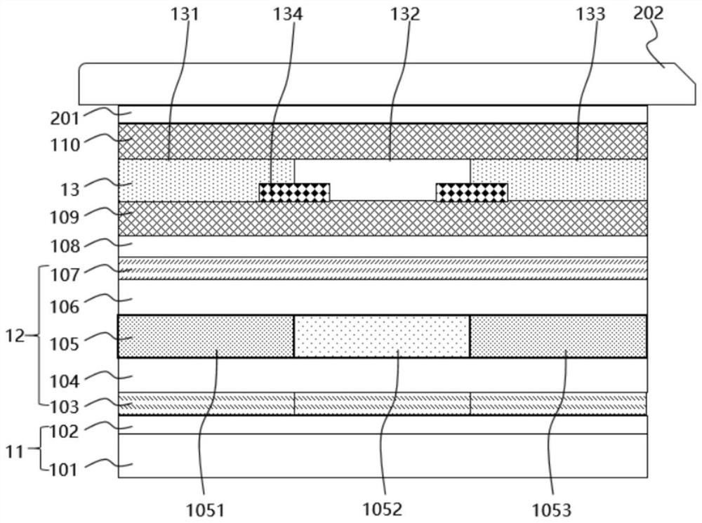
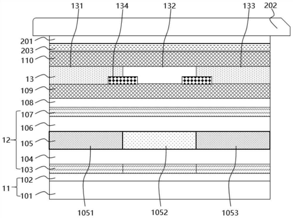
[0034] see figure 1 , figure 1 It is a schematic diagram of a first structure of a display panel 100 provided in an embodiment of the present application.
[0035] The embodiment of the present application provides a display panel 100. The display panel 100 includes an array substrate 11, a light-emitting device layer 12, and a color-resist layer 13. The light-emitting device layer 12 is disposed on the array substrate 11. The light-emitting device layer 12 includes a red light-emitting device 1052 , the first blue light emitting device 1051, the second blue light emitting device 1053; the color resistance layer 13 is disposed on the light emitting device layer 12, and the color resistance layer 13 includes a red color resistance 132, a blue color resistance 131, and a green color conversion unit 133; Wherein, the red color resistance 132 is set corresponding to the red light emitting device 1052, the blue color resistance 131 is set corresponding to the first blue light emit...
Embodiment 2
[0056] This embodiment is the same or similar to the above embodiments, except that the structure of the display panel 100 is further described.
[0057] In some embodiments, the color resistance layer 13 further includes a spacer layer 134 , the spacer layer 134 includes a plurality of openings 1341 , and the red color resistance 132 , the blue color resistance 131 and the green color conversion unit 133 are disposed between the spacer layers 134 .
[0058] Specifically, such as figure 1 As shown, the spacer layer 134 includes a plurality of openings 1341 , and the red color resist 132 , the blue color resister 131 and the green color conversion unit 133 are disposed on the openings 1341 of the spacer layer 134 .
[0059] Specifically, the opening of the spacer layer 134 is used to accommodate the red color resistance 132, the blue color resistance 131 and the green color conversion unit 133, and the spacer layer 134 separates the red color resistance 132, the blue color resi...
Embodiment 3
[0065] This embodiment is the same or similar to the above embodiments, except that the structure of the display panel 100 is further described.
[0066] In some embodiments, the display panel 100 further includes a first encapsulation layer 110 , and the first encapsulation layer 110 is disposed on a side of the color resist layer 13 away from the light emitting device layer 12 .
[0067] Specifically, the first encapsulation layer 110 is arranged on the surface of the color-resist layer 13, which can protect the color-resist layer 13, and can also prevent water vapor and oxygen from entering the light-emitting device layer 12 of the display panel 100, so as to avoid the life of the display panel 100. decline.
[0068] Specifically, the first encapsulation layer 110 may include an inorganic material layer, an organic material layer, or a multi-layer laminated structure of an inorganic material layer and an organic material layer.
[0069] In some embodiments, the display pan...
PUM
| Property | Measurement | Unit |
|---|---|---|
| thickness | aaaaa | aaaaa |
Abstract
Description
Claims
Application Information
 - Generate Ideas
- Intellectual Property
- Life Sciences
- Materials
- Tech Scout
- Unparalleled Data Quality
- Higher Quality Content
- 60% Fewer Hallucinations
Browse by: Latest US Patents, China's latest patents, Technical Efficacy Thesaurus, Application Domain, Technology Topic, Popular Technical Reports.
© 2025 PatSnap. All rights reserved.Legal|Privacy policy|Modern Slavery Act Transparency Statement|Sitemap|About US| Contact US: help@patsnap.com