
Data reading method of non-volatile memory array with pairing structure

A non-volatile storage and data reading technology, applied in the storage field, can solve problems such as exceptions, information reading errors, data changes, etc.

Active Publication Date: 2022-03-11
杭州领开半导体技术有限公司
View PDF13 Cites 2 Cited by
  • Summary
  • Abstract
  • Description
  • Claims
  • Application Information

AI Technical Summary

Problems solved by technology

Although a single voltage applied to the word line has little influence on the data stored in the memory tube, in practical applications, the data stored in the same memory array is generally read multiple times, for example, one hundred thousand to one million The number of times data is read, and the small interference generated by each read will accumulate gradually with the increase of the number of reads, which may eventually cause changes or abnormalities in the data stored in the storage array, resulting in the read data and The stored data is inconsistent, and information reading errors occur. This phenomenon is usually called "Read Disturb" in the field of non-volatile memory.

Method used


Image

  • Data reading method of non-volatile memory array with pairing structure
  • Data reading method of non-volatile memory array with pairing structure
  • Data reading method of non-volatile memory array with pairing structure

Examples


Embodiment Construction

[0024] Before the introduction of the data reading method of the non-volatile storage array with group pair structure of the present invention. Firstly, the non-volatile storage array with group-pair structure is introduced.

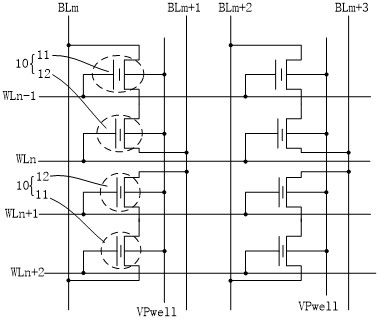
[0025] figure 1 It is an architectural diagram of a non-volatile storage array with a pair structure. Such as figure 1 As shown, the non-volatile memory array includes multiple pairs of memory cells 10 arranged in rows and columns, and the pairs of memory cells 10 in the same column correspond to the same two bit lines (Bit Line, BL); each of the The pair storage unit 10 includes a pair of first storage tubes 11 and second storage tubes 12 arranged in a column direction, the sources of the first storage tubes 11 and the second storage tubes 12 are connected, and the The drain of the first storage tube 11 is connected to one of the corresponding two bit lines, and the drain of the second storage tube 12 is connected to the other corresponding one of th...


PUM


Abstract

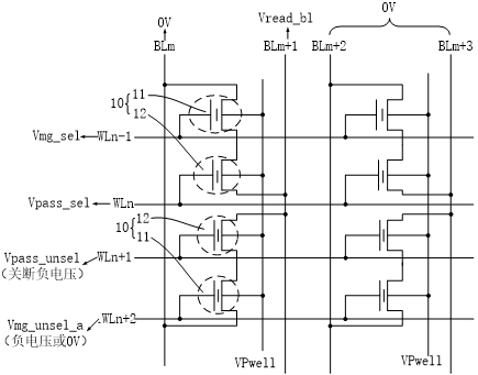
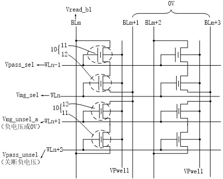
According to the data reading method of the non-volatile storage array with the pairing structure, in a first data reading period, zero-volt voltage is applied to a word line of a first storage tube of a selected storage unit, and starting voltage is applied to a word line of a second storage tube of the selected storage unit; a compensation positive voltage is applied to a word line of a first storage tube of a non-selected storage unit different from the selected storage unit, and a turn-off negative voltage is applied to a word line of a second storage tube of the non-selected storage unit; in a second data reading period, zero-volt voltage is applied to the word line of the second storage tube of the selected storage unit, turn-on voltage is applied to the word line of the first storage tube of the selected storage unit, compensation positive voltage is applied to the word line of the second storage tube of the non-selected storage unit, and turn-off negative voltage is applied to the word line of the first storage tube of the non-selected storage unit. Through the cooperation of the two data reading cycles, the soft erasure effect generated by turning off the negative voltage can be compensated by compensating the soft programming effect generated by the positive voltage, so that the probability of reading interference is reduced under the condition of not increasing additional circuits and reading cycle time.

Description

technical field [0001] The invention relates to the field of storage technology, in particular to a data reading method of a pair-structure non-volatile storage array. Background technique [0002] For a non-volatile (or non-volatile, Nonvolatile) semiconductor memory chip, after data is written, it can still maintain the stored data information even if it is powered off. Generally speaking, a non-volatile memory (that is, a non-volatile memory array) has a plurality of memory tubes arranged in rows and columns. In the process of actually reading non-volatile memory data, in order to identify the data stored in the selected storage tube, a voltage of corresponding magnitude is usually applied to the bit line of the selected storage tube or to both the bit line and the word line at the same time. Another word line voltage will be applied to the unselected memory tubes, and the voltages applied to the selected word lines and the unselected word lines will slightly interfere w...

Claims


Application Information

Patent Timeline
Patent Type & Authority Applications(China)
IPC IPC(8): G11C16/08G11C16/26G11C16/34
CPCG11C16/08G11C16/26G11C16/3404
Inventor 禹小军金波
Owner 杭州领开半导体技术有限公司
Learn More