Nested delay lock ring

A delay-locked ring and nesting technology, which is applied in the direction of automatic power control, electrical components, special data processing applications, etc., can solve the problem of increasing the total delay of the clock or signal path, etc.

Active Publication Date: 2022-03-04
SUZHOU POWERLINK MICROELECTRONICS
View PDF10 Cites 0 Cited by
  • Summary
  • Abstract
  • Description
  • Claims
  • Application Information

AI Technical Summary

Problems solved by technology

The problem often encountered in the design of similar chips is: when using multiple independent delay locked loops (DLL: delay locked loop) to meet the system's synchronization requirements for clocks and signals, it increases the total number of clock or signal paths. time delay

Method used


Image

  • Nested delay lock ring
  • Nested delay lock ring
  • Nested delay lock ring

Examples


Embodiment Construction

[0025] The following will clearly and completely describe the technical solutions in the embodiments of the present invention with reference to the drawings in the embodiments of the present invention. Based on the embodiments of the present invention, all other embodiments obtained by persons of ordinary skill in the art without making creative efforts belong to the protection scope of the present invention.

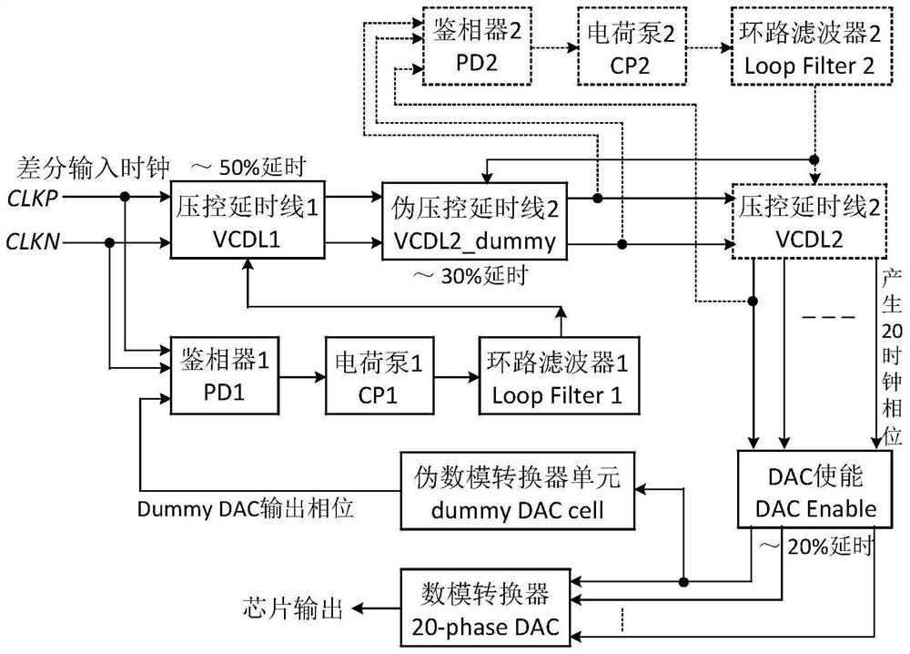
[0026] figure 1 It is a functional block diagram of the nested delay locked loop embodiment of the present invention. The function of the first delay-locked loop (DLL1) is to synchronize the output of the final 20-phase digital-to-analog converter (20-phase DAC) with the input differential clock (CLKP and CLKN), and the total loop delay is Minimum value, i.e. one clock cycle; In view of the fact that the actual DAC output cannot be directly used as phase feedback, the present invention uses the output of a matched dummy DAC cell (dummy DAC cell) to generate the feedbac...


PUM


Abstract

The invention discloses a nested delay locked loop, which belongs to the technical field of chip design, and comprises two mutually nested delay locked loops (DLL) in a chip circuit loop, the first delay locked loop (DLL1) can synchronize the output of a digital-to-analog converter (DAC) with an input differential clock (CLKP and CLKN), the second delay locked loop (DLL2) can generate a clock with the same frequency as the input differential clock (CLKN), and the first delay locked loop (DLL1) and the second delay locked loop (DLL2) can generate a clock with the same frequency as the input differential clock (CLKN). Therefore, the total delay of a chip circuit loop system clock or a signal path is minimized; according to the invention, the two delay locked loops (DLL) in the loop of the chip circuit are nested with each other, so that the synchronization requirements of respective loop clocks and signals are met, and the design goal of minimizing the total delay of the loop system of the chip circuit is achieved.

Description

technical field [0001] The invention belongs to the technical field of chip design, and in particular relates to a nested delay locked ring. Background technique [0002] In fields such as wired communication and large-scale digital circuits, clock synchronization and delay control are very important and difficult specialized techniques. With the continuous improvement of communication speed and digital processor frequency, especially when it involves signal and clock loops formed between different chips, the delay control of synchronous communication or digital calculation becomes more complex and challenging. [0003] As an application example of the present invention, while generating a multi-phase clock required by a digital-to-analog converter (DAC: digital-to-analog converter), it is also required that the DAC output is synchronized with the off-chip input clock. The problem often encountered in the design of similar chips is: when using multiple independent delay loc...

Claims


Application Information

Patent Timeline
Patent Type & Authority Applications(China)
IPC IPC(8): H03L7/23G06F30/33
CPCH03L7/235G06F30/33
Inventor 万海军李健平张跃玲
Owner SUZHOU POWERLINK MICROELECTRONICS
Why Eureka
Try Eureka