Regulation and control layer, preparation method and photoelectric device
An electrode and electric field technology, applied in the field of control layer and preparation, optoelectronic devices, can solve the problem of unadjustable refractive index of film layer
- Summary
- Abstract
- Description
- Claims
- Application Information
AI Technical Summary
Problems solved by technology
Method used
Image

Examples
preparation example Construction
[0063] The present application also provides a preparation method of the regulating layer, comprising:
[0064] B11. Providing a first electrode and a second electrode oppositely arranged.
[0065] B12, setting a solution containing charged or electrically polarizable nanoparticles on the first electrode and the second electrode.
[0066] B13, applying a voltage to the first electrode and the second electrode to form an electric field, and forming a control layer containing charged or electrically polarizable nanoparticles.
[0067] In the present application, a voltage is applied through the first electrode and the second electrode, so that an electric field is formed between the first electrode and the second electrode, and the charged or electrically polarizable nanoparticles are charged or electrically polarizable in a solvent to form an electric field containing A solution of charged or electrically polarizable nanoparticles, so that the accumulation degree of nanopartic...
Embodiment 1
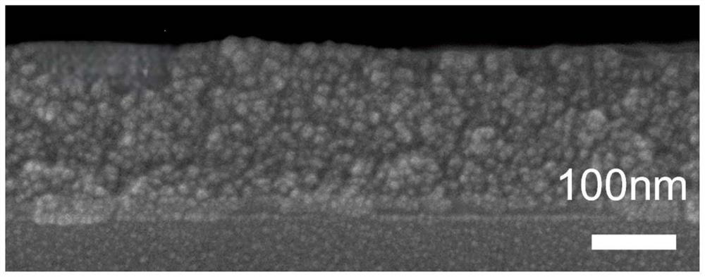
[0070] see Figure 5 and Figure 6 , Figure 5 It is a schematic flow chart of the preparation method of the control layer provided in the embodiment of the present application. Figure 6 It is a schematic flowchart of the first structure of the preparation method of the control layer provided in the embodiment of the present application. The present application also provides a method for preparing the control layer 10, including:
[0071]B11. Providing a first electrode and a second electrode oppositely arranged.
[0072] The materials of the first electrode and the second electrode are independently selected from one or more combinations of ITO, graphene, metal or transition metal chalcogenide. Transition metal chalcogenides including MoS 2 、MoSe 2 、WS 2 and WSe 2 one or a combination of several. The first electrode and the second electrode may be external electrodes or electrodes provided on the device.
[0073] B12, setting a solution containing charged or electr...
Embodiment 2
[0092] see Figure 10 , Figure 10It is a schematic flowchart of the second structure of the preparation method of the control layer provided in the embodiment of the present application.
[0093] It should be noted that the difference between embodiment 2 and embodiment 1 is:
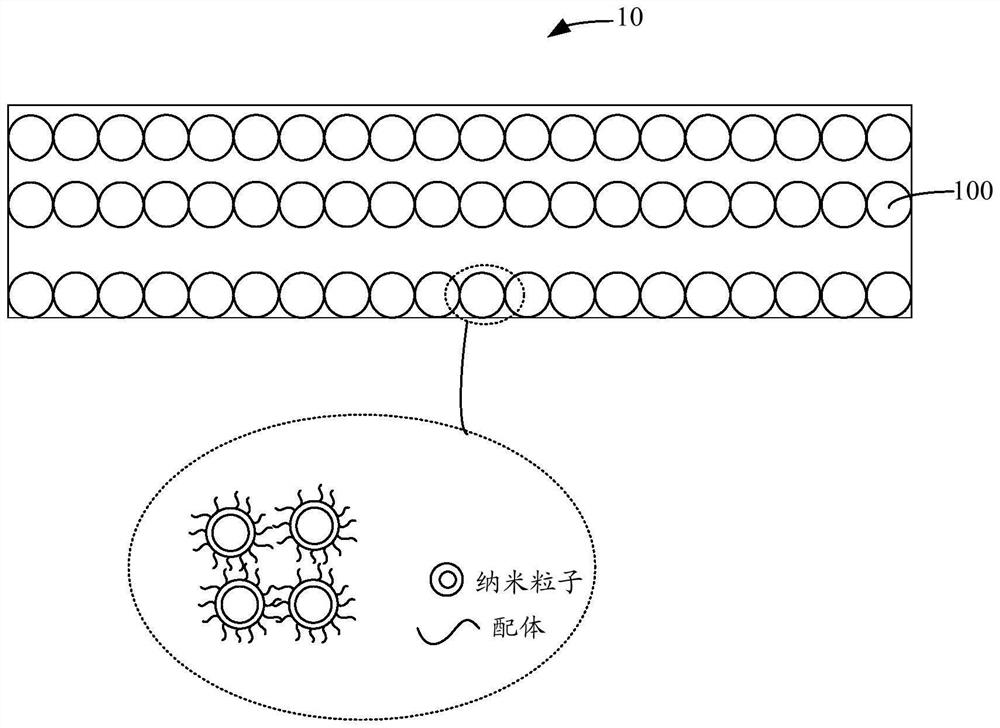
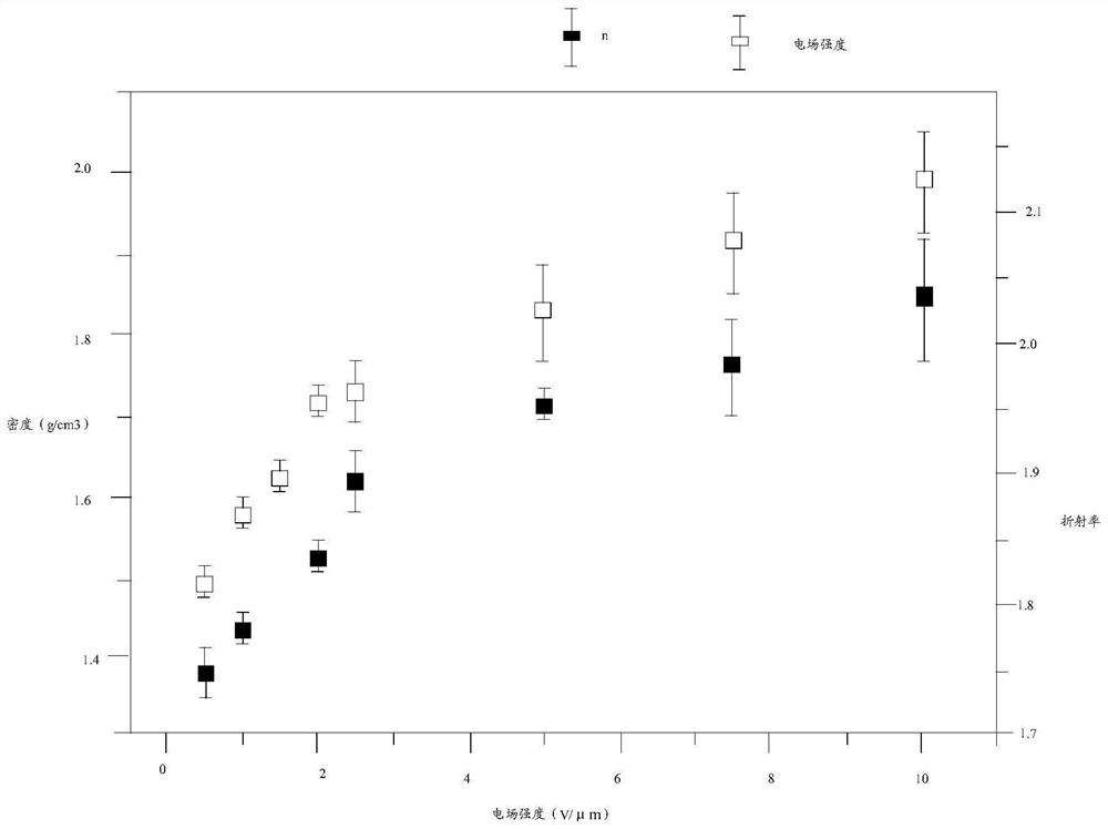
[0094] read on image 3 . Change the small voltage to a large voltage, that is, the large voltage is the second voltage; the small electric field is changed to a large electric field, that is, the large electric field is the second electric field, and the control layer 10 is formed, and the nanoparticles 100 are closely packed, that is, the nanoparticles 100 are in the Under the action of the large electric field, the refractive index of the control layer 10 changes from 1.5 to 2.4. .
[0095] Specifically, a large voltage is applied to the first electrode and the second electrode to form a large electric field, and the nanoparticles 100 are composed of CdSe / ZnS and the ligand as polyethylene glyc...
PUM
| Property | Measurement | Unit |
|---|---|---|
| density | aaaaa | aaaaa |
| density | aaaaa | aaaaa |
| density | aaaaa | aaaaa |
Abstract
Description
Claims
Application Information
 - Generate Ideas
- Intellectual Property
- Life Sciences
- Materials
- Tech Scout
- Unparalleled Data Quality
- Higher Quality Content
- 60% Fewer Hallucinations
Browse by: Latest US Patents, China's latest patents, Technical Efficacy Thesaurus, Application Domain, Technology Topic, Popular Technical Reports.
© 2025 PatSnap. All rights reserved.Legal|Privacy policy|Modern Slavery Act Transparency Statement|Sitemap|About US| Contact US: help@patsnap.com