Organic light emitting device and method for manufacturing organic light emitting device

A technology of organic light-emitting devices and organic light-emitting layers, which is applied in the manufacture of semiconductor/solid-state devices, electric solid-state devices, semiconductor devices, etc., and can solve the problems of diffuse reflection, OLED appearance influence, coupling-out efficiency limitation, etc.

Active Publication Date: 2016-05-18
OSRAM OLED
View PDF5 Cites 0 Cited by
  • Summary
  • Abstract
  • Description
  • Claims
  • Application Information

AI Technical Summary

Problems solved by technology

However, these method approaches for light outcoupling have significant disadvantages: the outcoupling efficiency is limited to approximately 60% to 70% of the light guided in the substrate, and the appearance of the OLED is significantly affected, since by the applied layers or Thin film creates a milky, diffuse reflective surface
However, these methodological pathways have so far not been implemented commercially in OLED products.

Method used


Image

  • Organic light emitting device and method for manufacturing organic light emitting device
  • Organic light emitting device and method for manufacturing organic light emitting device
  • Organic light emitting device and method for manufacturing organic light emitting device

Examples


Embodiment Construction

[0166] In the exemplary embodiments and figures, elements that are identical, of the same type or have the same effect can each be provided with the same reference numerals. The illustrated elements and their mutual size relationships are not to be regarded as to scale, rather individual elements such as layers, Components, devices and areas.

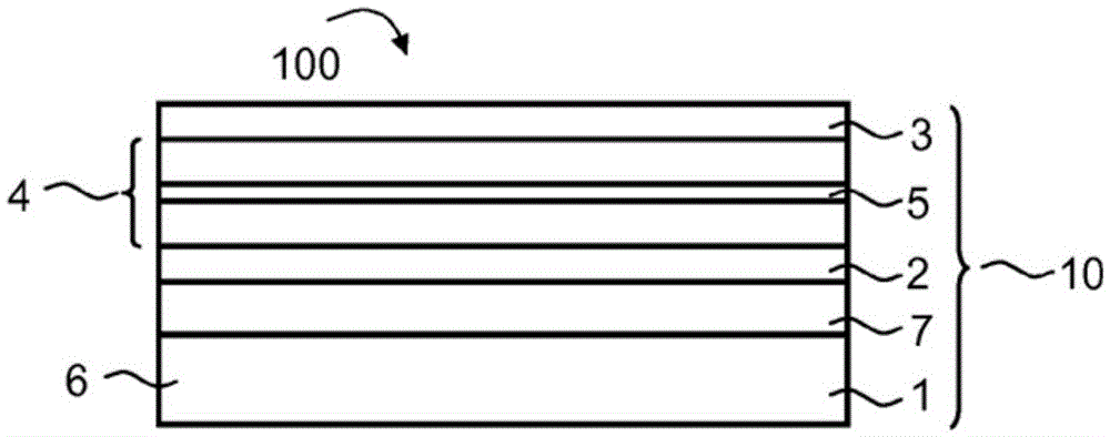
[0167] exist figure 1 An example of an organic light-emitting component 100 having a functional layer stack 10 is shown in FIG.

[0168] The functional layer stack 10 has a substrate 1 on which an organic functional layer stack 4 is arranged between a first electrode 2 and a second electrode 3 . The organic functional layer stack 4 has an organic emitting layer 5 .

[0169] In the exemplary embodiment shown, the substrate 1 is transparent, for example in the form of a glass pane or glass layer. A first electrode 2 is applied above the substrate, which first electrode comprises, for example, a transparent conductive oxide such as ITO...


PUM


Abstract

An organic light-emitting device is proposed having a functional layer stack (10), said functional layer stack having: a substrate (1); a first electrode (2) above said substrate; An organic functional layer stack (4), the organic functional layer stack has an organic light-emitting layer (5); and a second electrode (3) above the organic functional layer stack, wherein the layer (1) of the functional layer stack (10) , 2, 3) forming a carrier layer (6) for a scattering layer (7), wherein the scattering layer (7) has at least one first organic component and a second organic component (71, 72) having a refractive index different from each other, wherein the first organic component (71) is hydrophobic and the second organic component (72) is hydrophilic, wherein the glass transition temperature of the mixture of the first organic component (71) and the second organic component (72) is higher than room temperature , and wherein the first organic component (71) and the second organic component (72) exist partially separately in the scattering layer (7) and the scattering layer between the first organic component and the second organic component (71, 72) ( 7) A mesoscopic boundary layer ( 75 ) or scattering layer ( 7 ) is present as an intermediate phase ( 78 ) with a first organic component and a second organic component ( 71 , 72 ). Furthermore, a method for producing an organic light-emitting device is proposed.

Description

technical field [0001] An organic light emitting device and a method for manufacturing the organic light emitting device are proposed. Background technique [0002] In organic light-emitting diodes (OLEDs), only a part of the generated light is directly coupled out. The rest of the light generated in the active region is distributed onto different loss channels, for example into light absorbed in the substrate and light guided in the substrate, in the transparent electrodes and in the organic layer by waveguide effects and Surface plasmons that can be generated in metal electrodes. The waveguide effect results in particular from differences in the refractive index at the boundary surfaces between the individual layers and regions of the OLED. Typically, in known OLEDs only about a quarter of the light generated in the active region is coupled out into the surroundings, that is to say for example into air, while about 25% of the light generated % is lost due to waveguides ...

Claims


Application Information

Patent Timeline
Patent Type & Authority Patents(China)
IPC IPC(8): H01L51/52H01L51/00
CPCH10K85/151H10K50/854H10K50/85H10K50/30H10K50/865H10K71/40
Inventor 尼纳·里格尔蒂洛·罗伊施丹尼尔·斯特芬·塞茨
Owner OSRAM OLED
Why Eureka
Try Eureka