
LED display module and manufacturing method

A technology for display modules and manufacturing methods, applied to identification devices, instruments, semiconductor devices, etc., can solve the problems of high design difficulty, large product size, and low product yield, so as to reduce design difficulty, reduce finished product size, The effect of reducing the number of pads

Active Publication Date: 2022-03-04
HCP TECH CO LTD
View PDF19 Cites 1 Cited by
  • Summary
  • Abstract
  • Description
  • Claims
  • Application Information

AI Technical Summary

Problems solved by technology

At present, displays based on RGB LED light sources generally arrange multiple packaged RGB LED light sources directly on the display substrate. Compared with white LEDs, due to the number of pins ( There are many six pins), therefore, it is necessary to set up multiple solder pads on the display substrate, and since the driving lines of all RGB LED light sources must be arranged on the display substrate, a higher number of layers for the display substrate is proposed. Requirements, in this way, for the PCB circuit design of the display substrate, the design difficulty is relatively high, and the structure is complex, the product quality is relatively low, and the product size is relatively large

Method used


Image

  • LED display module and manufacturing method
  • LED display module and manufacturing method
  • LED display module and manufacturing method

Examples


Embodiment Construction

[0042] In order to describe the technical content, structural features, achieved goals and effects of the present invention in detail, the following will be described in detail in conjunction with the embodiments and accompanying drawings.

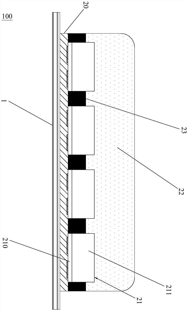
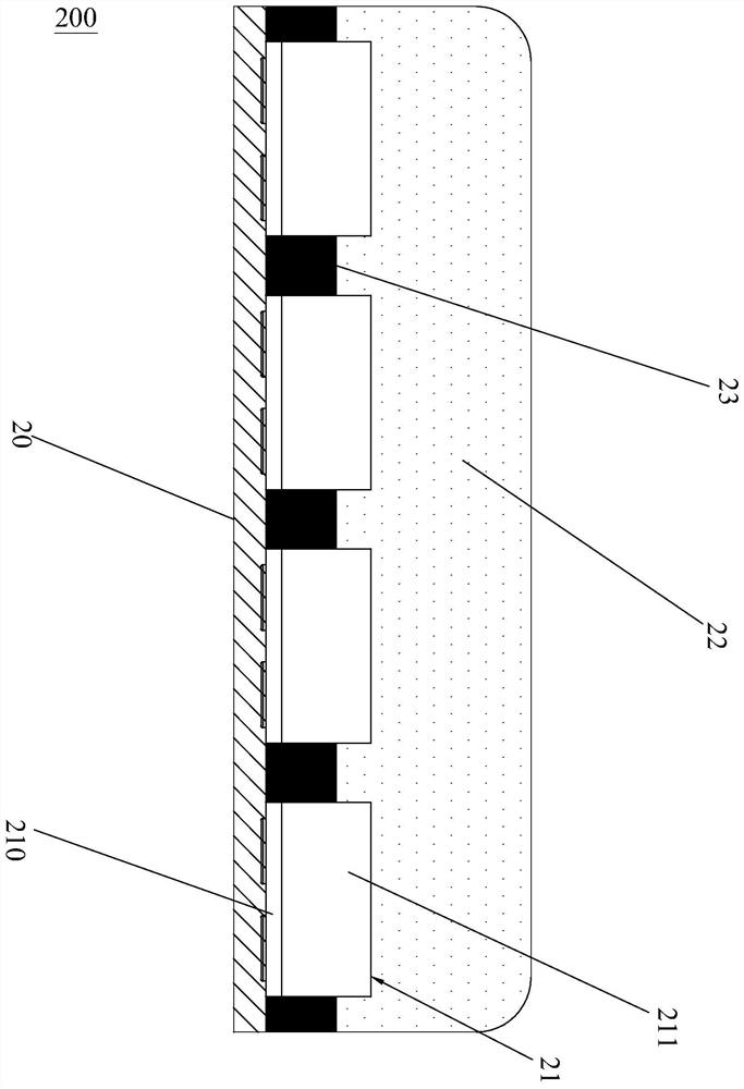
[0043] like figure 1 and figure 2 , this embodiment discloses an LED display module 100 based on an LED light source, which includes a display substrate 1 and an encapsulation module 200 disposed on the display substrate 1, the encapsulation module 200 includes a module substrate 20, several single-pixel packages body 21 and an outer encapsulation layer 22 , the outer encapsulation layer 22 is used to encapsulate several single-pixel encapsulation bodies 21 on the module substrate 20 .

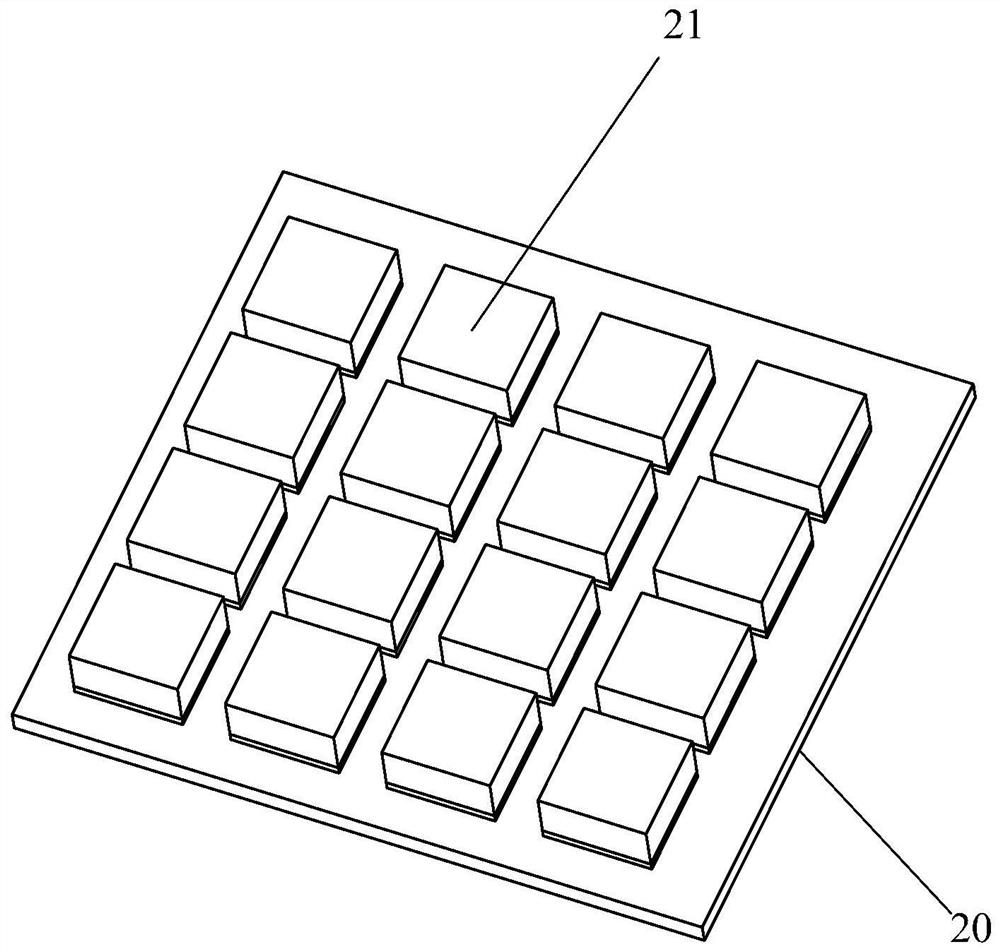
[0044] Please refer to figure 1 , figure 2 , Figure 4 and Figure 5 The single-pixel package 21 includes a unit substrate 210, a plurality of light-emitting chips, and an inner packaging layer 211. The inner packaging layer 211 is used to package a...


PUM


Abstract

The invention discloses an LED display module and a manufacturing method, and the manufacturing method comprises the steps: enabling a plurality of light-emitting chips to be packaged on a unit substrate, forming a single-pixel packaging body, and enabling the plurality of light-emitting chips to share a cathode or an anode on the unit substrate in the single-pixel packaging body; packaging the plurality of single-pixel packaging bodies on a module substrate to obtain a packaging module comprising the plurality of single-pixel packaging bodies, and on the packaging module, the plurality of single-pixel packaging bodies share an anode or a cathode; arranging the packaging module on a display substrate to obtain a display module; in the invention, the display module is obtained by two times of packaging, the single-pixel packaging bodies are formed by one time of packaging, and the display module is obtained by packaging a plurality of single-pixel packaging bodies again by the second time of packaging, so that the number of bonding pads on the display substrate can be effectively reduced, the design difficulty of a PCB (Printed Circuit Board) is reduced, and the size of a finished product of the display module is reduced.

Description

technical field [0001] The invention relates to the technical field of LED display, in particular to an LED display module and a manufacturing method. Background technique [0002] The RGB LED light source is based on the principle of three primary colors (red, green, blue). The three light-emitting chips R, G, and B are packaged together, and the three light-emitting chips R, G, and B emit light together to form the desired mixed light effect, such as White light, yellow light, etc. At present, displays based on RGB LED light sources generally arrange multiple packaged RGB LED light sources directly on the display substrate. Compared with white LEDs, due to the number of pins ( There are many six pins), therefore, it is necessary to set up multiple solder pads on the display substrate, and since the driving lines of all RGB LED light sources must be arranged on the display substrate, a higher number of layers for the display substrate is proposed. Requirements, in this wa...

Claims


Application Information

Patent Timeline
Patent Type & Authority Applications(China)
IPC IPC(8): H01L33/00H01L33/38H01L33/52G09F9/33
CPCH01L33/005H01L33/52H01L33/387G09F9/33H01L2933/0016H01L2933/005
Inventor 李星袁楚仁王周坤
Owner HCP TECH CO LTD
Learn More