Display substrate and display device

A technology for display substrates and substrates, used in semiconductor devices, electrical components, circuits, etc., can solve the problems of pixel shrinkage and brightness attenuation, and achieve the effect of avoiding brightness and avoiding large attenuation.

Pending Publication Date: 2022-03-01
BOE TECH GRP CO LTD +1
View PDF0 Cites 0 Cited by
  • Summary
  • Abstract
  • Description
  • Claims
  • Application Information

AI Technical Summary

Problems solved by technology

2. Root cause analysis, such as figure 2 as shown, figure 2 A schematic diagram of a partial cross-sectional structure of a display substrate for some technologies, when using UV light ( figure 2 Indicated by the dotted line with the arrow) after long-time irradiation, the pixel defining layer (PDL, material such as polyimide series organic matter) 32 will volatilize water and oxygen ( figure 2 Indicated by a dotted circle), the material of the organic light-emitting layer 36 is sensitive to water and oxygen, and the material of the organic light-emitting layer 36 will fail after absorbing the water and oxygen volatilized by the PDL layer 32. The central position is extended, which eventually causes the pixels to shrink, causing brightness attenuation

Method used


Image

  • Display substrate and display device
  • Display substrate and display device
  • Display substrate and display device

Examples


Embodiment Construction

[0043] Those skilled in the art should understand that the technical solutions of the embodiments of the present disclosure can be modified or equivalently replaced without departing from the spirit and scope of the technical solutions of the embodiments of the present disclosure, and should be covered by the claims of the present disclosure.

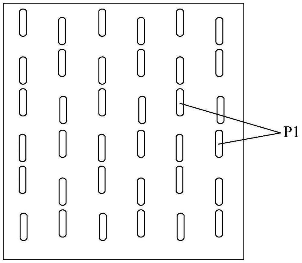
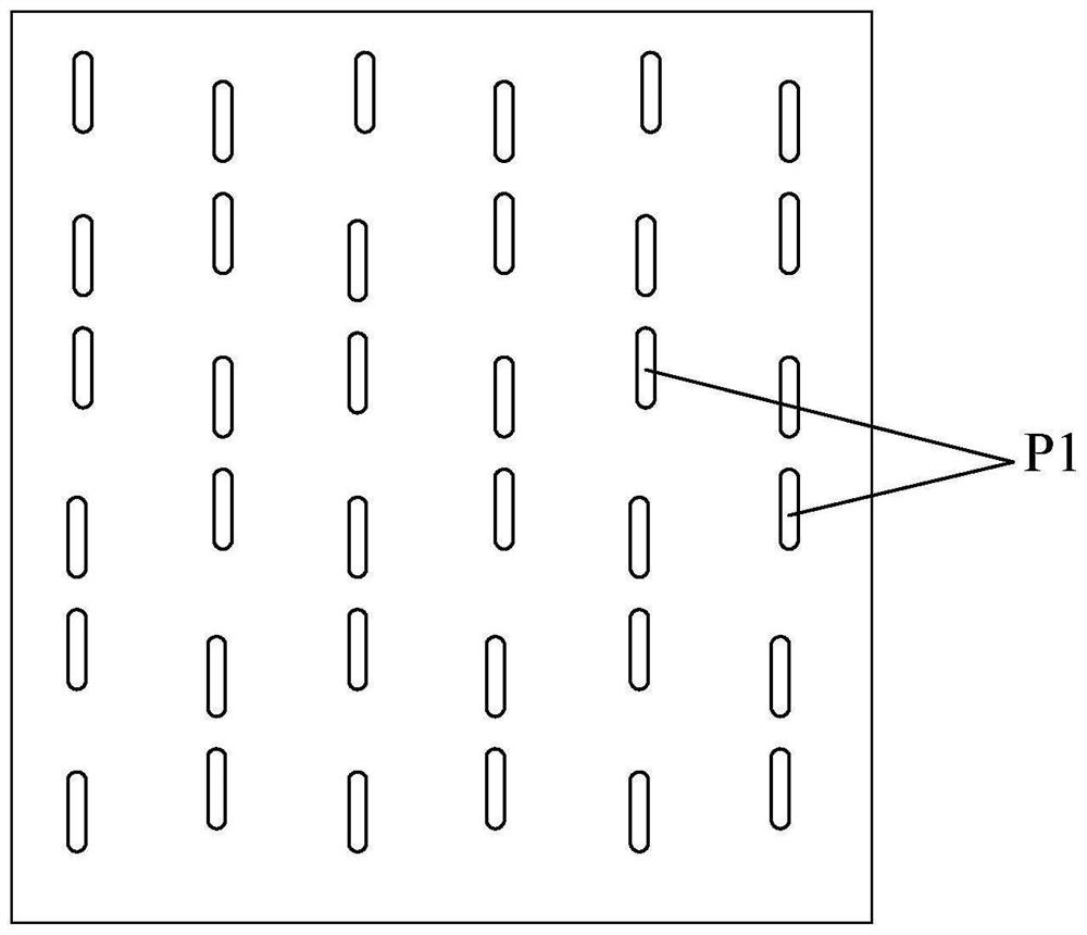
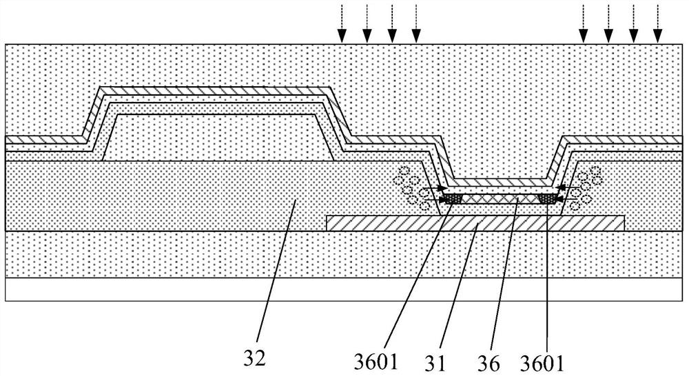
[0044] An embodiment of the present disclosure provides a display substrate, including a driving structure layer and a light emitting structure layer stacked on a substrate in sequence, the driving structure layer includes a pixel driving circuit; the light emitting structure layer includes a first electrode layer, a pixel defining layer , a water-oxygen barrier layer, an organic functional layer, and a second electrode layer; the first electrode layer includes a plurality of first electrodes disposed on the driving structure layer, and the pixel defining layer is disposed on the plurality of first electrodes A side of the electrode away...


PUM


Abstract

The invention discloses a display substrate and a display device, the display substrate comprises a driving structure layer and a light-emitting structure layer which are sequentially stacked on a substrate, and the light-emitting structure layer comprises a first electrode layer, a pixel defining layer, a water-oxygen barrier layer, an organic functional layer and a second electrode layer; the first electrode layer comprises a plurality of first electrodes arranged on the driving structure layer, the pixel defining layer is arranged on the sides, away from the substrate, of the first electrodes and provided with a plurality of first pixel openings, and each first pixel opening exposes the surface, away from the substrate, of the corresponding first electrode; the water oxygen barrier layer is at least partially arranged on the circumferential side wall of the first pixel opening; the organic functional layer comprises an organic light-emitting layer, and the organic functional layer and the second electrode layer are sequentially stacked on the side, away from the substrate, of the first electrode. The display substrate provided by the embodiment of the invention can prevent water and oxygen volatilized by the pixel defining layer from invading the organic light-emitting layer.

Description

technical field [0001] Embodiments of the present disclosure relate to the field of display technology, and in particular to a display substrate and a display device. Background technique [0002] Some organic light-emitting diode (OLED) display products need to be sold to high-altitude areas, where ultraviolet (UV light) radiation is relatively strong, and customers will evaluate the impact of UV radiation on electronic products. Taking a certain model product as an example, when the module screen is on, debug the Normal W255 screen, and test the initial brightness L0 at T0; When testing T580h, the brightness is L580h, L580h / L0<80%, that is, the brightness drops significantly. [0003] The above problems are analyzed as follows: 1. Phenomena analysis, after the module screen is continuously irradiated with UV light for 580 hours, the RGB (red, green and blue) pixels shrink to varying degrees. Taking the B pixel (that is, the blue sub-pixel P1) as an example, the light-...

Claims


Application Information

Patent Timeline
IPC IPC(8): H01L51/52H01L27/32
CPCH10K59/12H10K50/84
Inventor 包征王明强陈功胡宏锦杨皓天张家祥郝晓东王康张燚左堃傅晓亮张斌
Owner BOE TECH GRP CO LTD
Why Eureka
Try Eureka