Numerical design method of adiabatic mode coupler

A mode coupling and design method technology, applied in the direction of instruments, optical components, optics, etc., can solve the problems of complex structure and difficult processing, and achieve the effect of simple structure, speed up and saving computing memory

Active Publication Date: 2022-03-01
NANTONG UNIVERSITY
View PDF2 Cites 0 Cited by
  • Summary
  • Abstract
  • Description
  • Claims
  • Application Information

AI Technical Summary

Problems solved by technology

The existing design of thermal insulation devices is based on the analytical solution of equations, which usually requires some assumptions and approximations, and has a complex structure and is not easy to process.

Method used


Image

  • Numerical design method of adiabatic mode coupler
  • Numerical design method of adiabatic mode coupler
  • Numerical design method of adiabatic mode coupler

Examples


Embodiment Construction

[0024] The present invention will be further explained below in conjunction with the accompanying drawings.

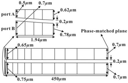
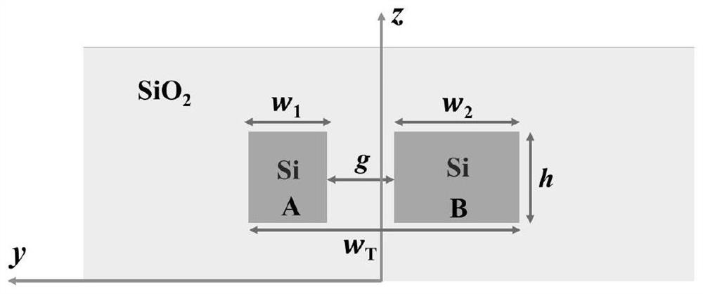
[0025] The present invention illustrates the design process by using an adiabatic mode coupler fabricated on a silicon waveguide plate on a silicon thin film substrate. A schematic diagram of an adiabatic mode coupler is shown in figure 1 and 2 As shown, it involves two waveguides, waveguide A and waveguide B placed next to each other. The cross-section of an adiabatic mode coupler as figure 1 Shown, where the height of the silicon waveguide h = 0.3μm. The widths of the two silicon waveguides are denoted as w 1 and w 2 , the gap width between the waveguides is marked g, and the optical wavelength is 1.55 μm.

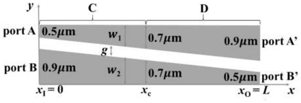
[0026] Such as figure 2 As shown, the width w of the two waveguides 1 and w 2 gradually changes along the propagation direction x, at one end of the coupler, that is, the input plane x = x I = 0, the waveguide of one silicon waveguide is narrower and t...


PUM


Abstract

The invention discloses a numerical design method of an adiabatic mode coupler, which comprises the following steps of: performing non-uniform segmentation on the adiabatic mode coupler along a light beam mode propagation direction, performing fine segmentation on a region sensitive to mode change, and for a region far away from a fine structure, as the mode change is gentle, the mode change is more stable, and the mode change is more stable. According to the method and the system, excessive fine segmentation does not need to be adopted, so that the purpose of carefully describing a local fine structure is achieved, the calculation amount is kept in a proper range, the calculation memory is saved, and the simulation design speed is increased. Moreover, the same loss constraint value is selected for each segment, and the adiabatic mode coupler which is small in size, easy to process, large in bandwidth and simple in structure is realized in a numerical mode.

Description

technical field [0001] The invention relates to a numerical design method of an adiabatic mode coupler. Background technique [0002] Silicon waveguides based on SOI structures have attracted widespread attention due to their fabrication compatibility with Complementary Metal Oxide Semiconductor (CMOS) processes, good mode confinement and enhanced nonlinearity. Waveguides in different devices are usually designed with different cross-sections to achieve different functions. Adiabatic couplers provide the connection for these devices. Adiabatic couplers consist of two waveguides that are close enough that the partial fields of their respective optical modes overlap each other. The power of the beam in one waveguide can be partially or fully coupled into the other waveguide, which is the photonic integration. The "connector" that connects various optical functional units in the circuit will play an important role in future large-scale photonic integrated chips. [0003] When...

Claims


Application Information

Patent Timeline
Patent Type & Authority Applications(China)
IPC IPC(8): G02B27/00
CPCG02B27/0012
Inventor 梁图禄荣巍巍吴钢雄
Owner NANTONG UNIVERSITY
Why Eureka
Try Eureka