Method and device for judging particle defect source in semiconductor manufacturing process

A particle defect and process technology technology, used in semiconductor/solid-state device testing/measurement, image data processing, instruments, etc., can solve the problems of low efficiency and error in particle defect source judgment, improve timeliness and avoid human errors Effect

Pending Publication Date: 2022-02-01
SHANGHAI HUALI MICROELECTRONICS CORP
View PDF0 Cites 0 Cited by
  • Summary
  • Abstract
  • Description
  • Claims
  • Application Information

AI Technical Summary

Problems solved by technology

[0003] The object of the present invention is to provide a method and device for judging the source of particle defects in the semi

Method used


Image

  • Method and device for judging particle defect source in semiconductor manufacturing process
  • Method and device for judging particle defect source in semiconductor manufacturing process
  • Method and device for judging particle defect source in semiconductor manufacturing process

Examples


Embodiment Construction

[0026] The metal wire digging structure and method proposed by the present invention will be further described in detail below in conjunction with the accompanying drawings and specific embodiments. Advantages and features of the present invention will be apparent from the following description and claims. It should be noted that all the drawings are in a very simplified form and use imprecise scales, and are only used to facilitate and clearly assist the purpose of illustrating the embodiments of the present invention.

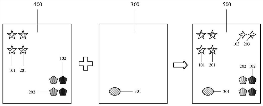
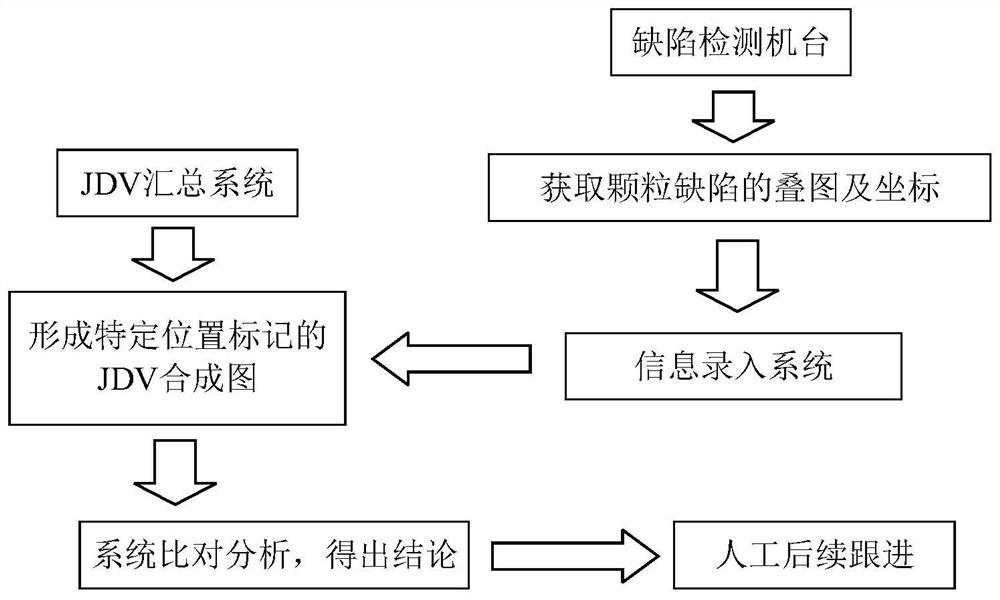
[0027] Please refer to Figure 1 to Figure 3 , an embodiment of the present invention provides a method for judging the source of particle defects in a semiconductor manufacturing process, including:

[0028] Step 710, please refer to figure 1 , in the wafer photolithography process, the JDV pattern 100 of the NMOS region and the JDV pattern 200 of the PMOS region of the photoresist layer in the ion implantation region are extracted, respectively compared w...


PUM


Abstract

The invention provides a method and device for judging a particle defect source in a semiconductor manufacturing process, and the method comprises the steps: extracting a JDV pattern of an NMOS region and a JDV pattern of a PMOS region of a photoetching layer of an ion implantation region in a wafer photoetching process, respectively carrying out the comparison with a plurality of layers of JDV patterns with opposite development, and generating two groups of JDV graphs with respective specific positions through the same parameter, and fitting the two groups of JDV graphs together to form a JDV fitting graph; extracting the JDV pattern of the ion implantation layer; fitting the JDV fitting graph and the JDV graph of the ion implantation layer together to form a JDV composite graph, and marking the specific position of the JDV graph of each layer; scanning a wafer through a defect detection machine to obtain particle defect information, comparing the obtained overlay of the particle defect with the JDV composite graph, and determining the source of the particle defect according to the mark of the particle defect in the overlay falling into the specific position of the JDV composite graph. The method has the advantages of rapidness, high efficiency and accuracy.

Description

technical field [0001] The invention relates to the technical field of semiconductor integrated circuits, in particular to a method and device for judging the source of particle defects in a semiconductor manufacturing process. Background technique [0002] Particulate pollutants come from a wide range of sources in the semiconductor manufacturing process, most of which come from the process flow, measurement process or machine hardware. However, there are also some particles due to problems in the process or long waiting time between processes. The small residues on the wafer surface gradually become larger after the deposition process at the post station, forming obvious particle defects. Such defects generally have a fixed location. specific characteristics. Taking the semiconductor manufacturing process of 55nm process as an example, this type of particle defect is mainly caused by the long waiting time from dry etching (Dry Etch) to wet etching (Wet Etch), and the loca...

Claims


Application Information

Patent Timeline
IPC IPC(8): G06T7/00G06T5/50G06T7/62H01L21/66
CPCG06T7/001G06T5/50G06T7/62H01L22/12H01L22/20G06T2207/30148G06T2207/20221
Inventor 雷涛
Owner SHANGHAI HUALI MICROELECTRONICS CORP
Why Eureka
Try Eureka