
Mask group, evaporation device and method for monitoring thicknesses of functional layers of light-emitting device

A technology for light-emitting devices and functional layers, which is applied to the monitoring of the thickness of the functional layer of the vapor deposition device and the light-emitting device, and the field of mask sets. time, improve work efficiency

Pending Publication Date: 2022-01-21
JITRI INST OF ORGANIC OPTOELECTRONICS CO LTD
View PDF0 Cites 0 Cited by
  • Summary
  • Abstract
  • Description
  • Claims
  • Application Information

AI Technical Summary

Problems solved by technology

[0004] An embodiment of the present invention provides a method for monitoring the thickness of a mask plate set, an evaporation device, and a functional layer of a light-emitting device, so as to solve the problem that the calibration and inspection process of the existing evaporation film layer thickness is relatively time-consuming.

Method used


Image

  • Mask group, evaporation device and method for monitoring thicknesses of functional layers of light-emitting device
  • Mask group, evaporation device and method for monitoring thicknesses of functional layers of light-emitting device
  • Mask group, evaporation device and method for monitoring thicknesses of functional layers of light-emitting device

Examples


Embodiment Construction

[0040] In order to make the purpose, technical solutions and advantages of the present invention clearer, the technical solutions of the present invention will be clearly and completely described through implementation with reference to the accompanying drawings in the embodiments of the present invention. Obviously, the described embodiments are the embodiment of the present invention. Some, but not all, embodiments. All other embodiments obtained by those skilled in the art based on the basic concepts disclosed and suggested by the embodiments of the present invention belong to the protection scope of the present invention.

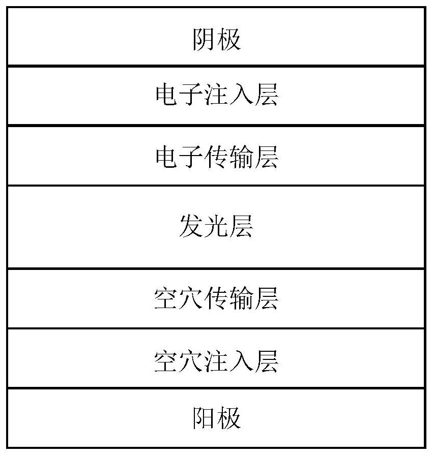
[0041] In the current OLED industry, Fine Metal Mask (FMM) technology is usually used to regionalize and pattern the evaporation material. During the evaporation process, a fixed mask and a moving substrate are used to evaporate Plated luminescent devices. figure 1 is a schematic structural diagram of a light emitting device provided by an embodiment o...


PUM


Abstract

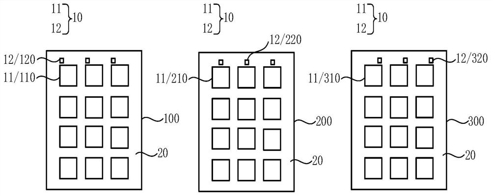
The embodiment of the invention discloses a mask group, an evaporation device and a method for monitoring the thicknesses of functional layers of a light-emitting device. The light-emitting device comprises the first functional layer to the Nth functional layer, and the mask group comprises a first mask to an Nth mask; the ith mask comprises an ith light-transmitting part and an ith shading part, the ith light-transmitting part comprises an ith functional layer opening and an ith functional layer monitoring opening, the ith functional layer opening is used for forming the ith functional layer through evaporation, the ith functional layer monitoring opening is used for forming an ith functional layer monitoring area through evaporation, the ith functional layer monitoring area is used for monitoring the evaporation thickness of the ith functional layer, and i is larger than or equal to 1 and smaller than or equal to N; and the vertical projections of the functional layer openings of any two masks in the mask group on the to-be-masked plane are at least partially overlapped, and the vertical projections of the functional layer monitoring openings of any two masks on the to-be-masked plane are at most partially overlapped. By adopting the mask group, film thickness calibration and troubleshooting of different stations can be realized, consumed time is short, and the working efficiency is high.

Description

technical field [0001] The embodiments of the present invention relate to the technical field of evaporation, and in particular to a mask set, an evaporation device, and a method for monitoring the thickness of a functional layer of a light-emitting device. Background technique [0002] Organic Light-Emitting Diode (OLED for short) uses organic light-emitting materials. When powered on, the device emits light automatically. It has a series of advantages such as low power consumption, wide color gamut, high brightness, and high response, so it has gradually become the mainstream. For lighting and flat panel display technology, major manufacturers at home and abroad are also vigorously deploying in the OLED industry, which further promotes the development of the OLED industry. [0003] In the technical process of OLED device preparation, the glass substrate is usually bonded through a mask, and then the device is patterned by evaporation. During the evaporation process, chang...

Claims


Application Information

Patent Timeline
IPC IPC(8): C23C14/04C23C14/24C23C14/54H01L51/56
CPCC23C14/042C23C14/24C23C14/545H10K71/164H10K71/166H10K71/00Y02E10/549
Inventor 陈汐王江南徐林帅张川李文重
Owner JITRI INST OF ORGANIC OPTOELECTRONICS CO LTD
Learn More