Connecting part, consumable chip, electronic imaging equipment and method for installing connecting part and consumable container

A technology of electronic imaging and consumable containers, which is applied to the parts, connections, fixed/insulated contact members of the connection device, etc., which can solve problems such as memory damage, voltage rise, and user operation troubles

Active Publication Date: 2022-01-21
ZHUHAI TIANWEI TECH DEV CO LTD
View PDF11 Cites 3 Cited by
  • Summary
  • Abstract
  • Description
  • Claims
  • Application Information

AI Technical Summary

Problems solved by technology

Usually, it often takes a few milliseconds from detecting that the level of the detection terminal 21 is too high to disconnecting the power supply of the high-voltage terminal 25, which may cause damage to the memory
In addition, once the detection terminal 21 is abnormal, or the detection circuit is abnormal, and the high-voltage terminal 25 and the connection terminal 26 are not detected in time when the high-voltage terminal 25 is short-circuited, it is easy to cause the memory to be loaded with an excessively high voltage for a long time and cause storage damage. Therefore, the substrate The main cause of memory damage is that the power terminal on the 20 is loaded with excessive voltage
[0021] In addition, due to the short distance between the detection terminals 21, 24 and the high-voltage terminals 25, 29, it is easy to cause false detection problems. The connection terminal 26 may still not be short-circuited, but in this case, the control circuit 30 will still judge that an abnormal situation occurs, and send an abnormal alarm, which will affect the normal operation of the inkjet printer
[0022] The Chinese utility model patent with the publication number CN201856448U discloses a chip and an inkjet printer. Memory, this chip is provided with a plurality of connection terminals electrically connected with the chip main control circuit board 33, and when in use, the chip 18 is inserted in the printing word cart 14, therefore, if the user replaces the ink cartridge 15 Failure to replace / reset the chip 18 in time will cause a mismatch between the ink volume data stored in the chip 18 and the remaining ink volume in the actual ink cartridge 15, especially after the ink cartridge has been replaced for many times, the cumulative difference of the ink volume data It will become bigger and bigger, which will cause trouble for users
[0023] In addition, the Chinese invention patent with the application number CN2021110631452 discloses a connector, a chip and an inkjet printer. Drops fall on the chip, resulting in damage to the memory. However, when installing this connector, the user needs to align the slot on the connector with the limit between the two character carriage units on the print carriage 14. Components, and this limit piece is generally relatively thin, user operation trouble; and, after installing the above-mentioned connecting piece, if the contacts on the connecting piece and the multiple contact pins of the contact pin adapter unit 36 ​​such as 41, 44, 45 , 49 electrical connection occurs, at this time, even if the ink cartridge is not installed, the printer will prompt that the ink cartridge has been installed in place, which will also cause trouble to the user

Method used


Image

  • Connecting part, consumable chip, electronic imaging equipment and method for installing connecting part and consumable container
  • Connecting part, consumable chip, electronic imaging equipment and method for installing connecting part and consumable container
  • Connecting part, consumable chip, electronic imaging equipment and method for installing connecting part and consumable container

Examples


no. 1 example

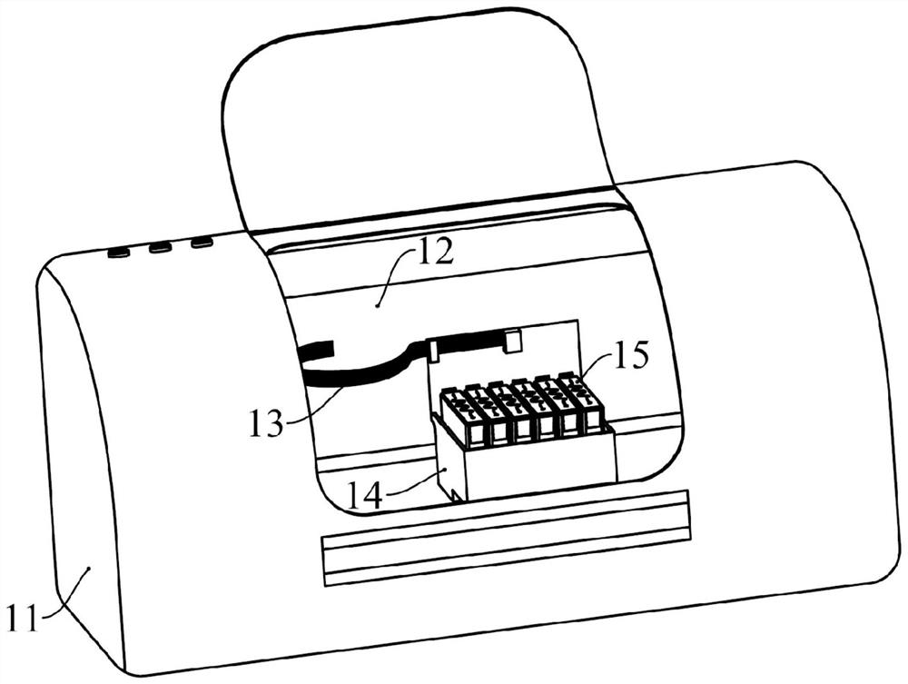
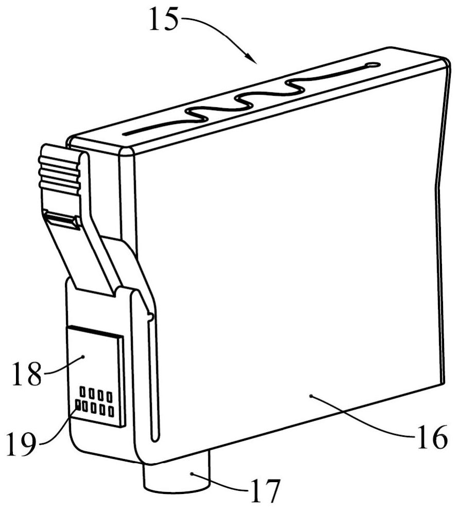
[0075] The electronic imaging device of this embodiment is an inkjet printer, which is provided with a body, and a printing carriage is formed in the body, see Figure 7 , a plurality of ink cartridges 610 are detachably installed in the printing carriage, each ink cartridge 610 has a housing, the housing surrounds a cavity containing ink, and an ink outlet communicating with the cavity is provided below the cavity , the ink in the cavity can flow out through the ink outlet. Moreover, an ink cartridge chip 621 is detachably mounted on an outer wall of the housing.

[0076] The ink cartridge chip 621 has a substrate, and a side of the substrate close to the printing carriage is provided with multiple connection terminals. Preferably, the multiple connection terminals are arranged in two rows. A memory is provided on the other side of the substrate, and the memory is a non-volatile memory such as EEPROM or FLASH. In this embodiment, the multiple connection terminals on the ink...

no. 2 example

[0104] It can be foreseen that, in the above-mentioned first embodiment, since the second functional contact for detecting whether a single color ink cartridge is installed in place and the second functional contact for detecting whether all color ink cartridges are installed in place are both arranged on the connecting member 640, and after the connector 640 is installed on the printing word cart 14, all the contact parts 670 on the wiring board 641 will be connected with the main control circuit of the chip due to the extrusion effect of the contact pin 38 on the contact pin transfer unit 36. The contacts of the corresponding functions on the board 33 are in electrical contact. Therefore, after the connector 640 is installed, even if no ink cartridges are installed, the inkjet printer will prompt that all color ink cartridges have been installed in place. In order to solve this problem, the present invention provides another kind of embodiment.

[0105] see Figure 19 , the...

no. 3 example

[0110] see Figure 20 , the connecting piece of this embodiment has a connecting plate 830, and the connecting piece is divided into four parts, namely a first part 841, a second part 842, a third part 843 and a fourth part 844, and two adjacent parts are provided with Each part is provided with an opening slot. In this embodiment, the structures of the four parts are completely the same, and the first part 841 is taken as an example for description below.

[0111] Only two first functional contact portions 8411 and 8414 are provided on the first portion 841 . Different from the second embodiment, the wiring board 830 of this embodiment does not provide a second functional contact portion and a second conductive portion. Moreover, the first conductive part includes a first switch K31 , and the first switch K31 is connected between the two first functional contact parts 8411 , 8414 . Therefore, the length of the connecting piece is set to be relatively short.

[0112] Theref...


PUM


Abstract

The invention provides a connecting part, a consumable chip, electronic imaging equipment and a method for installing the connecting part and a consumable container. The connecting part is arranged between a chip main control circuit board and a contact pin switching unit, contact portions are arranged on the connecting part and are electrically connected to contacts of the chip main control circuit board, the contact portions only comprise first functional contact portions and / or second functional contact portions, the first functional contact portions are electrically connected to first functional contacts corresponding to the chip main control circuit board, are detection contacts and are electrically connected through first conductive portions, the second functional contact portions are electrically connected to second functional contacts corresponding to the chip main control circuit board and are contacts for applying high-voltage signals, and the connecting part is arranged on the electronic imaging equipment. The invention further provides the method for installing the connecting part and the consumable container to the electronic imaging equipment. According to the connecting part, the consumable chip, the electronic imaging equipment and the method for installing the connecting part and the consumable container, the situation that a memory of the consumable chip is damaged due to loading of the high-voltage signals can be avoided.

Description

technical field [0001] The invention relates to the technical field of electronic imaging, in particular to a connector, a consumable chip and an electronic imaging device, and also to a method for installing the connector and the consumable container. Background technique [0002] As common office equipment, electronic imaging equipment provides great convenience for modern office. Common electronic imaging equipment includes printers, copiers, etc. Existing printers are divided into inkjet printers and laser printers. Inkjet printers use ink The ink cartridge used as the ink cartridge ejects ink to the paper to form the text or pattern to be printed on the paper; the laser printer uses the toner cartridge containing the toner as the ink cartridge to form the text or pattern to be printed on the medium. [0003] see figure 1 , an existing color inkjet printer has a casing 11, figure 1 The inkjet printer is shown with the chassis 11 omitted. The machine core 12 of ink-jet...

Claims


Application Information

Patent Timeline
Patent Type & Authority Applications(China)
IPC IPC(8): B41J2/175B41J2/01H01R13/40H01R13/629
CPCB41J2/1752B41J2/17553B41J2/1753B41J2/01H01R13/40H01R13/629
Inventor 文冠果张强罗寿杰
Owner ZHUHAI TIANWEI TECH DEV CO LTD
Why Eureka
Try Eureka