Shielding assembly of semiconductor equipment and reaction chamber

A reaction chamber and semiconductor technology, applied in ion implantation plating, metal material coating process, coating, etc., can solve the problems of uneven wafer temperature, poor film uniformity, and inability to achieve heat dissipation, so as to improve uniformity , increase production capacity, and increase the effect of a single working time

Pending Publication Date: 2022-01-07
BEIJING NAURA MICROELECTRONICS EQUIP CO LTD
View PDF6 Cites 0 Cited by
  • Summary
  • Abstract
  • Description
  • Claims
  • Application Information

AI Technical Summary

Problems solved by technology

[0004] However, when the escaped metal atoms diffuse and bombard the wafer in the reaction chamber, they will also bombard the pressure ring, and the contact area between the pressure ring, the lining and the deposition ring is small, and effective heat dissipation cannot be achieved. During the continuous process, a large amount of heat will be accumulated, and the heat accumulated by the pressure ring will radiate to the wafer, so that during the process, the temperature of the edge of the wafer near the pressure ring is significantly higher than that of the wafer far away from the pressure ring The temperature of the center of the wafer causes the temperature of the wafer to be uneven during the process, resulting in poor uniformity of the film prepared on the wafer

Method used


Image

  • Shielding assembly of semiconductor equipment and reaction chamber
  • Shielding assembly of semiconductor equipment and reaction chamber
  • Shielding assembly of semiconductor equipment and reaction chamber

Examples


Embodiment Construction

[0031] In order for those skilled in the art to better understand the technical solution of the present invention, the shielding assembly and the reaction chamber of the semiconductor device provided by the present invention will be described in detail below with reference to the accompanying drawings.

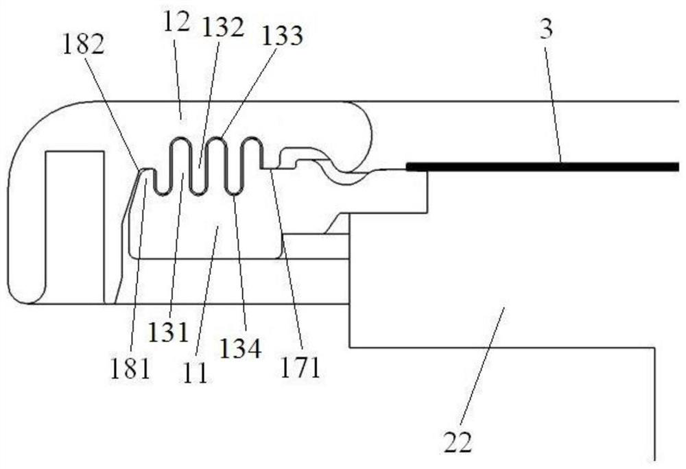
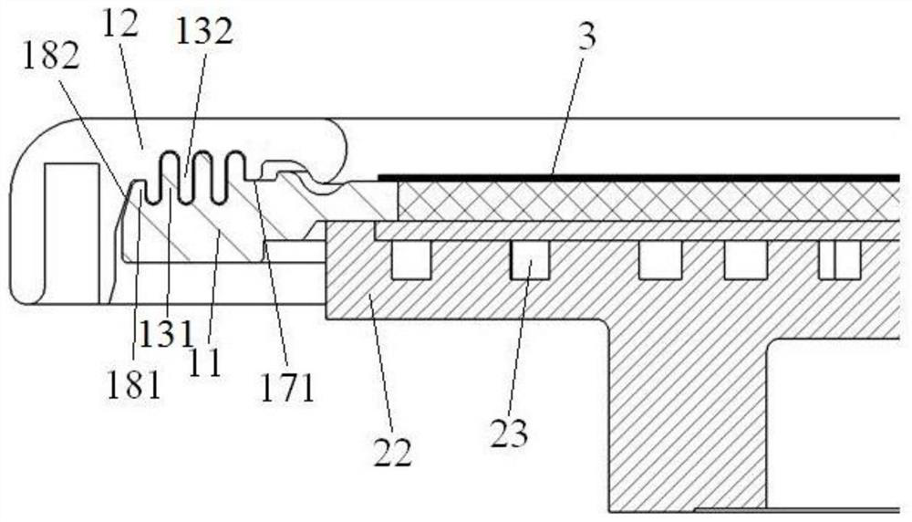
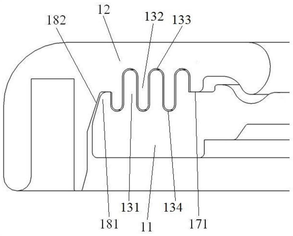
[0032] Such as figure 1 and Figure 7 As shown, the embodiment of the present invention provides a shielding assembly for a semiconductor device, which is arranged in a reaction chamber. The shielding assembly includes a first ring body 11 and a second ring body 12. The first ring body 11 is used to surround the reaction chamber On the outer peripheral wall of the carrier part 22, the second ring body 12 is movably arranged on the lining 27 in the reaction chamber, and the second ring body 12 is located above the first ring body 11, the first ring body 11 and The second ring body 12 can be selectively separated or abutted, and the two surfaces of the first ring body 11 and th...


PUM


Abstract

The invention provides a shielding assembly of semiconductor equipment and a reaction chamber. The shielding assembly of the semiconductor equipment is arranged in the reaction chamber and comprises a first ring body and a second ring body, and the first ring body is used for surrounding the peripheral wall of a bearing part in the reaction chamber; the second ring body is movably arranged on a lining in the reaction chamber, the second ring body is located above the first ring body, and the first ring body and the second ring body can be selectively separated from each other or abut against each other. The shielding assembly of the semiconductor equipment is characterized in that heat exchange structures which can be matched with each other are correspondingly arranged on two surfaces, which abut against each other, of the first ring body and the second ring body, and the heat exchange structures are used for transferring heat on the second ring body to the first ring body when the first ring body abuts against the second ring body. The heat of the second ring body is quickly transferred to the first ring body, so that the heating rate of the second ring body can be slowed down, the uniformity of a deposited film is improved, the single working time of the second ring body is prolonged, and the productivity is further improved.

Description

technical field [0001] The present invention relates to the technical field of semiconductor equipment, in particular to a shielding assembly and a reaction chamber of a semiconductor equipment. Background technique [0002] A physical vapor deposition (Physical Vapor Deposition, PVD for short) process can deposit a thin film on a wafer. The existing method of depositing thin films on wafers by magnetron sputtering is to ionize the reaction gas in the reaction chamber to form plasma, and attract the plasma to bombard the target, so that the metal atoms of the target escape from the target. Thin films are deposited on the wafer by bombarding the wafer with the help of the escaped metal atoms diffusing in the reaction chamber. [0003] In order to prevent the escaped metal atoms from diffusing to the inner wall of the reaction chamber and being arranged on the carrier part for carrying the wafer in the reaction chamber, polluting the inner wall of the reaction chamber and the...

Claims


Application Information

Patent Timeline
IPC IPC(8): C23C14/35C23C14/54
CPCC23C14/35C23C14/541
Inventor 李新颖王宽冒
Owner BEIJING NAURA MICROELECTRONICS EQUIP CO LTD
Why Eureka
Try Eureka