
Processing method for improving interconnection and separation of through holes of PTFE circuit board

A processing method and technology of via holes, which are applied in the processing of insulating substrates/layers, printed circuits, and printed circuit manufacturing, etc., can solve the problem of poor interconnection of holes and walls, the effect of removing glue is minimal, and affecting the stability of circuit board signal transmission, etc. question

Pending Publication Date: 2021-12-31
珠海杰赛科技有限公司 +2
View PDF6 Cites 0 Cited by
  • Summary
  • Abstract
  • Description
  • Claims
  • Application Information

AI Technical Summary

Problems solved by technology

[0003] In the production process of PTFE circuit boards, since PTFE is a thermoplastic material, drilling dirt and residual PTFE glue are prone to appear on the inner wall of the hole during the drilling process, and the chemical stability of PTFE is very high. The adhesive removal effect of the via hole of the board is negligible, and the residual PTFE glue at the via hole will cause poor interconnection of the hole wall and affect the stability of the signal transmission of the circuit board

Method used


Image

  • Processing method for improving interconnection and separation of through holes of PTFE circuit board

Examples


Embodiment 1

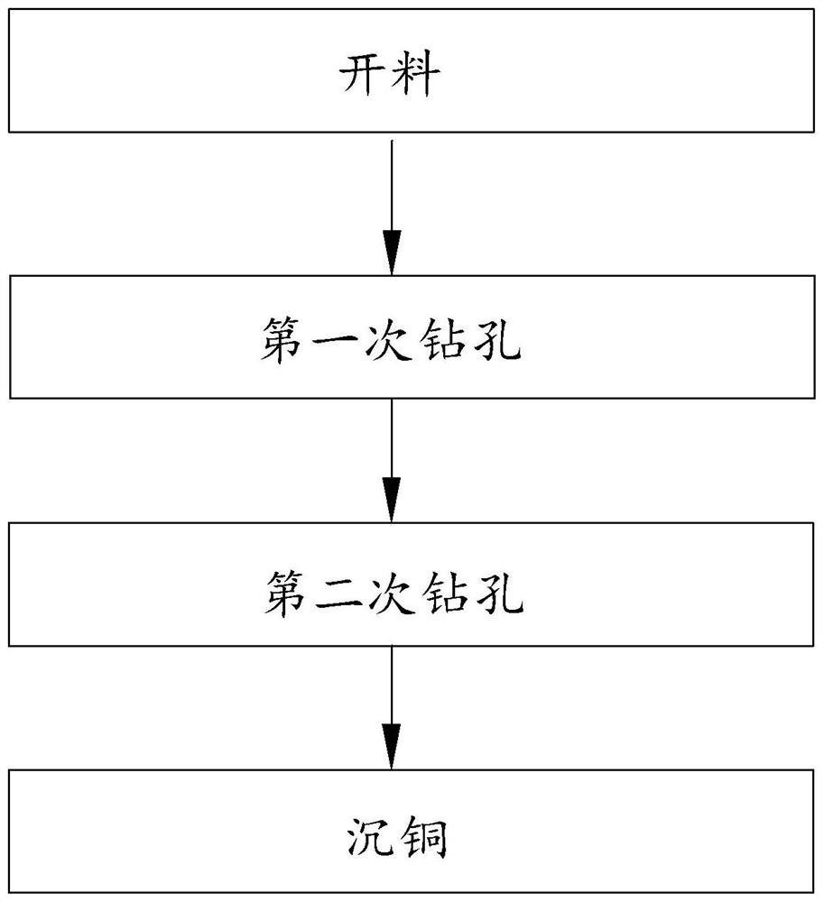
[0032] The present invention improves the processing method for the interconnection and separation of PTFE circuit board via holes, comprising the following steps:

[0033] Cutting: cutting the double-sided copper clad laminate, the middle layer of the double-sided copper clad laminate is a PTFE layer.

[0034] Drilling for the first time: select the first drill with a drill diameter of 0.25 mm, and drill the double-sided copper-clad laminate for the first time at a drilling speed of 80 kr / min to obtain via holes.

[0035] The second drilling: stop for 30 minutes, after the conduction hole is cooled, select the second drill bit with a diameter of 0.225mm, and drill the conduction hole for the second time at a drilling speed of 90kr / min to discharge the first drill Melt and fiberglass debris from holes.

[0036] Copper Immersion: First, use a plasma degumming machine to perform plasma degumming on double-sided copper-clad laminates. The temperature of plasma degumming is contr...

Embodiment 2

[0039] The present invention improves the processing method for the interconnection and separation of PTFE circuit board via holes, comprising the following steps:

[0040] Cutting: cutting the double-sided copper clad laminate, the middle layer of the double-sided copper clad laminate is a PTFE layer.

[0041] Drilling for the first time: select the first drill with a drill diameter of 0.35 mm, and drill the double-sided copper-clad laminate for the first time at a drilling speed of 100 kr / min to obtain via holes.

[0042] S4 second drilling: stop for 60 minutes, after the conduction hole is cooled, select the second drill bit with a diameter of 0.325mm, and drill the conduction hole for the second time at a drilling speed of 110kr / min to discharge the first time Melt and fiberglass debris from drilling.

[0043]Copper Immersion: First, use a plasma degumming machine to perform plasma degumming on double-sided copper-clad laminates. The temperature of the plasma degumming is...


PUM


Abstract

The invention discloses a processing method for improving interconnection and separation of through holes of a PTFE circuit board, and belongs to the technical field of PTFE circuit board manufacturing. The processing method for improving interconnection and separation of the through holes of the PTFE circuit board comprises the steps of cutting a double-sided copper-clad plate, wherein the middle layer of the double-sided copper-clad plate is a PTFE plate layer; selecting a first drilling tool, and drilling the double-sided copper-clad plate for the first time to obtain a via hole; stopping for 30-60 min, after the via hole is cooled, selecting a second drilling tool with the diameter smaller than that of the first drilling tool by 0.025 mm to conduct second drilling on the via hole, and discharging melt glue and glass fiber chips generated during first drilling; and firstly, carrying out plasma degumming on the double-sided copper-clad plate by using a plasma degumming machine, and then carrying out copper deposition on the double-sided copper-clad plate. By drilling the via hole again, the melt glue and glass fiber chips generated by drilling for the first time are discharged and prevented from being adhered to the hole wall to affect signal transmission.

Description

technical field [0001] The invention relates to the technical field of PTFE circuit board manufacturing, in particular to a processing method for improving the interconnection and separation of via holes of the PTFE circuit board. Background technique [0002] With the continuous development of communication technology, the signal transmission rate is getting faster and faster. Radar and antenna PCBs require substrate materials with small dielectric constant and low dielectric loss. Therefore, more and more PCB substrates of this type are made of PTFE. manufacture. [0003] In the production process of PTFE circuit boards, since PTFE is a thermoplastic material, drilling dirt and residual PTFE glue are prone to appear on the inner wall of the hole during the drilling process, and the chemical stability of PTFE is very high. The adhesive removal effect of the via hole of the board is negligible, and the residual PTFE glue at the via hole will lead to poor interconnection of ...

Claims


Application Information

Patent Timeline
Patent Type & Authority Applications(China)
IPC IPC(8): H05K3/00H05K3/42
CPCH05K3/0047H05K3/0055H05K3/42
Inventor 齐国栋邓勇刘国汉关志锋
Owner 珠海杰赛科技有限公司
Learn More