A mini-led driving method and display system
A driving method, mini-led technology, applied in static indicators, instruments, etc., can solve the problems of low service life, insufficient backlight area, low system stability, etc. Effect
- Summary
- Abstract
- Description
- Claims
- Application Information
AI Technical Summary
Problems solved by technology
Method used
Image
Examples
Embodiment 1
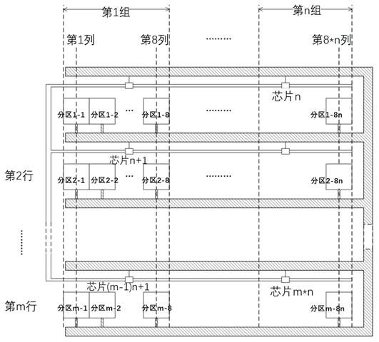
[0041] This embodiment discloses a Mini-LED dynamic backlight single-line driving method, which supports breakpoint resume transmission, such as figure 1 As shown, this method realizes the routing of a single-layer PCB board and the design of a chip by designing the PCB routing and making a special layout for the power supply and ground routing. Such as figure 1As shown, the Mini-LED includes m rows and n groups of chips. In this embodiment, each group of chips includes x columns, and each column corresponds to a partition, that is, each group includes x partitions, and m, n, and x are all natural numbers.
[0042] Starting from the first group of each row, the signals are transmitted corresponding to the partitions of the chip and transmitted to the corresponding chip of each partition, and m rows are copied based on this, so as to realize the area division of the number of chip rows * chip columns * number of partitions , for the convenience of description, this embodiment ...
Embodiment 2
[0052] When this embodiment supports MINI-LED dynamic backlight single-line drive for breakpoint resume transmission, the connection and driving mode of the chip to the partition is basically the same as that of Embodiment 1. The difference is that the pin design of the chip described in this embodiment is the same as that of Embodiment 1. Example 1 is different.
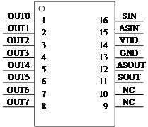
[0053] Image 6 Shown is a chip with an independent communication protocol involved in this embodiment. The chip has 8 partition-driven chips. PIN pins 1 to 8 are output ports OUT0 to OUT7, and PIN pin 16 is an input pin for resume transmission. ASIN, PIN 15 is the power supply VDD, PIN 14 is the data input SIN, PIN 13 is the ground GND, and PIN 12 is the data output SOUT. In this example, the breakpoint resume function is realized by transferring SOUT across chips.
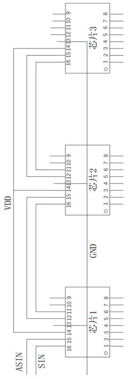
[0054] Figure 7 Shown is a schematic diagram of the connection between chips in this embodiment. According to the function of the chip and the PCB...
PUM
 Abstract
Description
Claims
Application Information
 - R&D
- Intellectual Property
- Life Sciences
- Materials
- Tech Scout
- Unparalleled Data Quality
- Higher Quality Content
- 60% Fewer Hallucinations
Browse by: Latest US Patents, China's latest patents, Technical Efficacy Thesaurus, Application Domain, Technology Topic, Popular Technical Reports.
© 2025 PatSnap. All rights reserved.Legal|Privacy policy|Modern Slavery Act Transparency Statement|Sitemap|About US| Contact US: help@patsnap.com


