Coating material and preparation method thereof
A film layer and base material technology, applied in the field of coating materials and its preparation, can solve the problems of differentiation of coating effects, difficulty in accurately adjusting optical constants, etc., and achieve the effect of reducing dull color
- Summary
- Abstract
- Description
- Claims
- Application Information
AI Technical Summary
Problems solved by technology
Method used
Image
Examples
preparation example Construction
[0061] Another embodiment of the present invention provides a method for preparing the coating material as described above, comprising the following steps:
[0062] Place the substrate under vacuum conditions, bombard the Nb target with an ion source, deposit and form a Nb layer on the surface of the substrate, and control the thickness of the Nb layer to ≥140nm;
[0063] Based on the Nb layer, bombarding the targets corresponding to the high-refraction layer and the target material corresponding to the low-refraction layer by ion bombardment and feeding auxiliary gas to form alternate high-refraction layers and low-refraction layers on the Nb layer.
[0064] In a preferred embodiment, the Nb layer, high or low refractive layer is formed using ion beam assisted deposition (IBAD), the target is made of the metal to be deposited, and oxygen or nitrogen is implanted into the target bombarded with the ion beam when required material combination. Therefore, the sputtering process ...
Embodiment 1
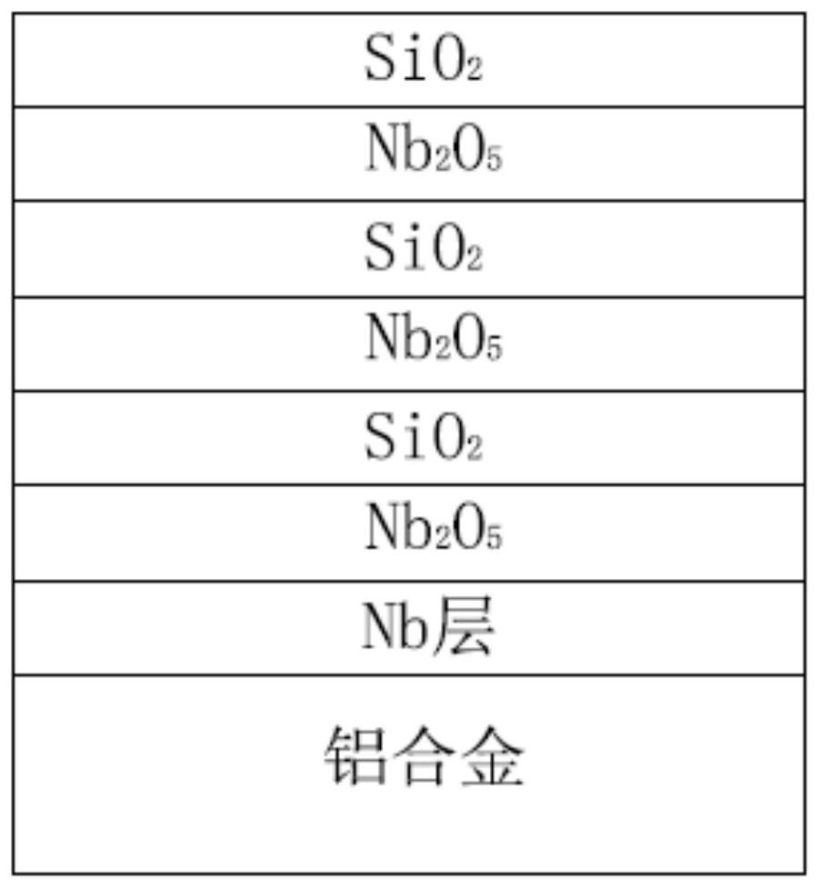
[0069] This embodiment is used to illustrate the coating material disclosed in the present invention and its preparation method, including the following steps:
[0070] SiO 2 Obtained by sputtering Si target coating method; elemental Nb and Nb 2 o 5 Obtained by sputtering Nb targets.
[0071] a. Put the aluminum alloy substrate on the fixture of the sputtering machine, and vacuumize;
[0072] b. The vacuum degree of the chamber to be coated reaches 3×10 -3 At Pa, pass in argon gas, and after the gas is stable, turn on the ion source, and perform ion cleaning on the surface of the substrate for 2 to 5 minutes;
[0073] c. The ion source continues to work, and at the same time turn on the sputtering power supply of the Nb target with a power of 10KW and a thickness of 184nm to complete the first coating of the Nb layer;
[0074] d. Turn on the oxygen of the ion source, the flow rate is 200sccm, continue to turn on the power supply of the Nb target, and deposit Nb 2 o 5 Th...
Embodiment 2
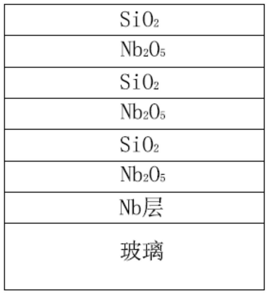
[0082] This embodiment is used to illustrate the coating material disclosed in the present invention and its preparation method, including most of the operating steps in Example 1, the difference being:
[0083] The base material is selected from glass, and the obtained coating materials such as figure 2 shown.
PUM
| Property | Measurement | Unit |
|---|---|---|
| thickness | aaaaa | aaaaa |
| thickness | aaaaa | aaaaa |
| thickness | aaaaa | aaaaa |
Abstract
Description
Claims
Application Information
 - R&D
- Intellectual Property
- Life Sciences
- Materials
- Tech Scout
- Unparalleled Data Quality
- Higher Quality Content
- 60% Fewer Hallucinations
Browse by: Latest US Patents, China's latest patents, Technical Efficacy Thesaurus, Application Domain, Technology Topic, Popular Technical Reports.
© 2025 PatSnap. All rights reserved.Legal|Privacy policy|Modern Slavery Act Transparency Statement|Sitemap|About US| Contact US: help@patsnap.com


