
Method for solving compatibility and adaptation of different chip pins

A pin configuration and pin technology, applied in the fields of instruments, electrical digital data processing, etc., can solve problems such as unanticipated special needs that are difficult to meet, chip application scenarios, and defects in chip function application scenarios, so as to reduce costs, The effect of improving utilization

Pending Publication Date: 2021-12-14
深圳市伦茨科技有限公司
View PDF4 Cites 1 Cited by
  • Summary
  • Abstract
  • Description
  • Claims
  • Application Information

AI Technical Summary

Problems solved by technology

1. With traditional integrated circuit technology, the chip function needs to be determined according to the expected product application scenario at the design stage, which limits the product to the expected designed function, and some unexpected special needs are difficult to meet
[0004] 2. The pin function of the chip is easy to be analyzed, and the product application scenarios of the chip have the risk of being copied
[0005] 3. In fact, all chips are defective in functional application scenarios

Method used


Image

  • Method for solving compatibility and adaptation of different chip pins
  • Method for solving compatibility and adaptation of different chip pins
  • Method for solving compatibility and adaptation of different chip pins

Examples


Embodiment 1

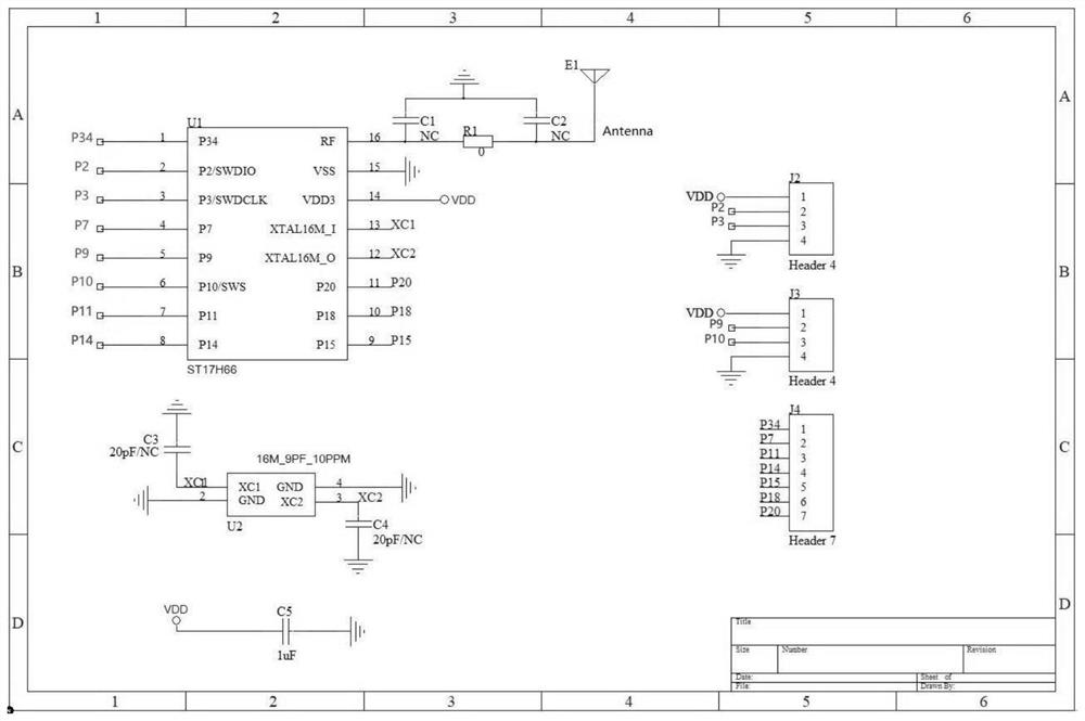
[0041] figure 1 The example chip structure diagram of the present invention is compatible with two kinds of chip pins.

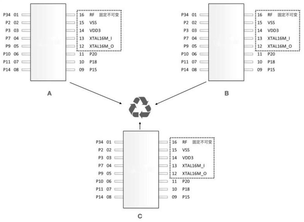
[0042] figure 2 A on the left side above is the pin configuration of the first type of chip, and B on the right side above is the pin configuration of the second type of chip. Using the method of c in the present invention, it can be packaged to be compatible with the first type of chip at the same time Two kinds of chips of chip A and the second type of chip B (lower part in the figure).

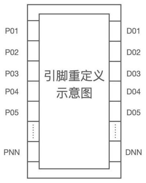
[0043] Such as image 3 P01, P02, and ~PNN shown represent the pin function positions of the chip. Under the control of the editable IO MUX function, the interface positions can be remade to achieve the effect that the chip pins are compatible and adapted.

[0044] Figure 4 Provide the logic structure diagram of IO MUX for the present invention, from P00 to P10, there are 11 configurable contacts in total. Peripheral module IOs mapping via IOMUX mapping. Periph...

Embodiment 2

[0051] In the following, in the programmable IO MUX function mode, the pins with the I2C bus interface mode are compatible and adapted to GPIO as an example to describe in detail.

[0052] The programmable IO MUX function is to provide a flexible I / O configuration, the ports of most peripheral devices can be configured and mapped to any physical I / O contacts (even die boundaries). Among them, peripheral modules include I2C 0-1, I2S, UART, PWM 0-5, SPI 0-1, quadrature decoder, etc. However, for other specific purpose peripherals, their IOs mapping is fixed when enabled, these special purpose peripherals include JTAG, analog_ios, GPIOs and key scan.

[0053] Such as Figure 5 The example chip structure diagram of the present invention is compatible with two kinds of chip pins.

[0054] Such as Figure 6 When described in specific implementation, configuration module is made up of GPIO configuration module, I2C bus configuration module and selector etc., wherein, GPIO configu...


PUM


Abstract

The invention provides a method for solving compatibility and adaptation of different chip pins. The method comprises the following steps of: setting pin configuration modes, and defining a corresponding total number of pin configuration modes according to the total number of chips needing pin compatibility; according to the pin configuration modes, redefining the positions of the pins under the control of an editable IO MUX function; and by controlling the editable IO MUX function, remaking an interface function definition to achieve compatibility and adaptation of the chip pins. According to the method of the invention, mode configuration is carried out on the pins of different chips, the pins of the chips can be defined and the positions of the pins of the chips can be configured again; the method can be compatible with various chip pins; chip resources can be utilized to the maximum extent; the utilization rate of the chips is improved, and the cost of the product is reduced.

Description

technical field [0001] The invention belongs to the field of integrated circuit design, in particular to a method for realizing compatibility and adaptation of different chip pins in a supply chain. Background technique [0002] With the rapid development of integrated circuit technology, the higher the integration level of the chip, one thousand manufacturers have one thousand kinds of chip products, corresponding to the application of different functions will choose different chips, and the position of the pin function definition in the chip will always be It is different. On the one hand, it is necessary to improve the differentiated competitiveness of chips in the subdivision field, and to meet the needs of customers for private customization of product applications. The pin must be different from competitors in the same industry; on the other hand, from From the perspective of research and development costs, if there is a chip that can meet the functional requirements o...

Claims


Application Information

Patent Timeline
Patent Type & Authority Applications(China)
IPC IPC(8): G06F13/38G06F13/40G06F13/42
CPCG06F13/387G06F13/4068G06F13/4282
Inventor 徐命波
Owner 深圳市伦茨科技有限公司
Learn More