Ultraviolet LED epitaxial structure and preparation method and application thereof
An epitaxial structure and ultraviolet technology, applied in electrical components, circuits, semiconductor devices, etc., can solve the problems of low luminous efficiency of devices and affect commercialization, and achieve the effect of improving internal quantum efficiency, improving balance, and improving luminous efficiency.
- Summary
- Abstract
- Description
- Claims
- Application Information
AI Technical Summary
Problems solved by technology
Method used
Image


Examples
Embodiment 1
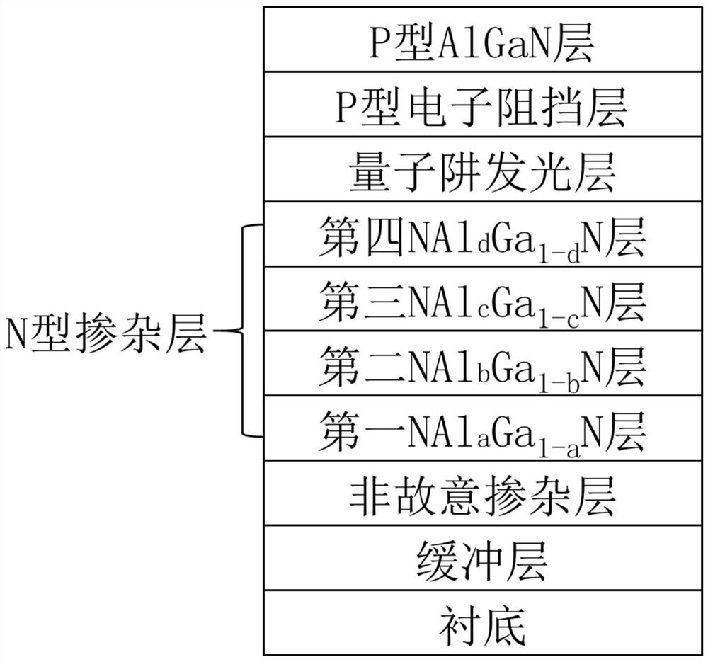
[0037] An ultraviolet LED epitaxial structure, including a substrate, a buffer layer, an unintentionally doped layer, an N-type doped layer, a quantum well light-emitting layer, a P-type electron blocking layer, and a P-type AlGaN layer from bottom to top; the N-type The doped layer sequentially includes the first NAl from bottom to top a Ga 1-a N layer, second NAl b Ga 1-b N layer, the third NAl c Ga 1-c N layer and fourth NAl d Ga 1-d N layers. Where a=0.1, b=0.25, c=0.15, d=0.2.
[0038] The preparation method of the ultraviolet LED epitaxial structure comprises the following steps:
[0039] Step S1: preparing a substrate;
[0040] Step S2: growing a buffer layer on the substrate; the growth temperature of the buffer layer is 800° C., and the growth thickness is 15 nm;
[0041] Step S3: growing an unintentionally doped layer on the buffer layer; the growth temperature of the unintentionally doped layer is 1100° C., and the growth thickness is 2.0 μm;
[0042] Ste...
Embodiment 2
[0047] An ultraviolet LED epitaxial structure, including a substrate, a buffer layer, an unintentionally doped layer, an N-type doped layer, a quantum well light-emitting layer, a P-type electron blocking layer, and a P-type AlGaN layer from bottom to top; the N-type The doped layer sequentially includes the first NAl from bottom to top a Ga 1-a N layer, second NAl b Ga 1-b N layer, the third NAl c Ga 1-c N layer and fourth NAl d Ga 1-d N layers. Where a=0.1, b=0.3, c=0.15, d=0.25.
[0048] The preparation method of the ultraviolet LED epitaxial structure comprises the following steps:
[0049] Step S1: preparing a substrate;
[0050] Step S2: growing a buffer layer on the substrate; the growth temperature of the buffer layer is 900° C., and the growth thickness is 50 nm;
[0051] Step S3: growing an unintentionally doped layer on the buffer layer; the growth temperature of the unintentionally doped layer is 1100° C., and the growth thickness is 4.0 μm;
[0052] Ste...
Embodiment 3
[0057] An ultraviolet LED epitaxial structure, including a substrate, a buffer layer, an unintentionally doped layer, an N-type doped layer, a quantum well light-emitting layer, a P-type electron blocking layer, and a P-type AlGaN layer from bottom to top; the N-type The doped layer sequentially includes the first NAl from bottom to top a Ga 1-a N layer, second NAl b Ga 1-b N layer, the third NAl c Ga 1-c N layer and fourth NAl d Ga 1-d N layers. Where a=0.15, b=0.3, c=0.2, d=0.25.
[0058] The preparation method of the ultraviolet LED epitaxial structure comprises the following steps:
[0059] Step S1: preparing a substrate;
[0060] Step S2: growing a buffer layer on the substrate; the growth temperature of the buffer layer is 800° C., and the growth thickness is 15 nm;
[0061] Step S3: growing an unintentionally doped layer on the buffer layer; the growth temperature of the unintentionally doped layer is 1100° C., and the growth thickness is 2.0 μm;
[0062] Ste...
PUM
| Property | Measurement | Unit |
|---|---|---|
| Thickness | aaaaa | aaaaa |
| Thickness | aaaaa | aaaaa |
| Thickness | aaaaa | aaaaa |
Abstract
Description
Claims
Application Information
 - R&D
- Intellectual Property
- Life Sciences
- Materials
- Tech Scout
- Unparalleled Data Quality
- Higher Quality Content
- 60% Fewer Hallucinations
Browse by: Latest US Patents, China's latest patents, Technical Efficacy Thesaurus, Application Domain, Technology Topic, Popular Technical Reports.
© 2025 PatSnap. All rights reserved.Legal|Privacy policy|Modern Slavery Act Transparency Statement|Sitemap|About US| Contact US: help@patsnap.com