Organic electroluminescent device and organic electroluminescent device

An electroluminescence device and electroluminescence technology, which are applied in the direction of electric solid devices, electrical components, semiconductor devices, etc., can solve the problems of low luminous brightness and color shift of red photonic pixels and green photonic pixels, and achieve the effect of increasing the control effect.

Active Publication Date: 2020-05-08
YUNGU GUAN TECH CO LTD
View PDF4 Cites 0 Cited by
  • Summary
  • Abstract
  • Description
  • Claims
  • Application Information

AI Technical Summary

Problems solved by technology

In practical applications, when the blue sub-pixel is turned on, although the voltage is mainly across the blue sub-pixel, due to the better conductivity of the common hole injection layer, part of the voltage will be applied to the green sub-pixel through the common hole injection layer. In the photo sub-pixel and / or the red sub-pixel, since the turn-on voltages of the red sub-pixel and the green sub-pixel are lower than the turn-on voltage of the blue sub-pixel, the red sub-pixel and / or the green sub-pixel are easy to be turned on at the same time
That is, in the case of low gray scale, the luminous brightness of the red sub-pixel and / or green sub-pixel cannot strictly meet the requirements to achieve the low-brightness display effect, and the low gray scale color cast (reddish) phenomenon occurs

Method used


Image

  • Organic electroluminescent device and organic electroluminescent device
  • Organic electroluminescent device and organic electroluminescent device
  • Organic electroluminescent device and organic electroluminescent device

Examples


Embodiment 1

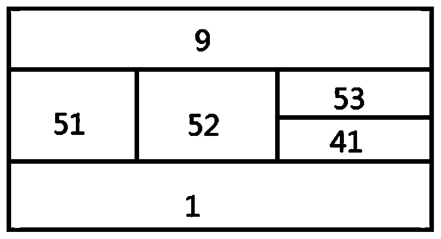
[0056] An embodiment of the present invention provides an organic electroluminescent device, such as Figure 4 As shown, it includes a first electrode layer 1, a hole injection layer 2, a hole transport layer 3, an electron blocking layer 4, a light emitting layer 5, a hole blocking layer 6, an electron transport layer 7, and an electron injection layer 8 stacked in sequence. As well as the second electrode layer 9, the light-emitting layer 5 includes a host material and a guest material, and the first carrier functional layer is an electron blocking layer 4, which is doped with a guest material.

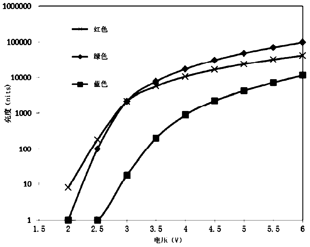
[0057] Wherein, the light emitting layer 5 is a red light emitting layer or a green light emitting layer, that is, this embodiment provides a red organic electroluminescent device and a green organic electroluminescent device;

[0058] The structure of the red light device is: ITO(100nm) / CuPc(20nm) / NPB(40nm) / TPD:Ir(piq) 3 (3%,65nm) / CBP:Ir(piq) 3 (3%, 30nm,) / NPB(5nm) / TPBi(40nm) / LiF...

Embodiment 2

[0061] The embodiment of the present invention provides an organic electroluminescent device, the structure of which is the same as that of embodiment 1, except that the hole blocking layer 6 is the second carrier functional layer, which is also doped with the guest material of the light emitting layer.

[0062] The structure of the red light device is: ITO(100nm) / CuPc(20nm) / NPB(40nm) / TPD:Ir(piq) 3 (3%,65nm) / CBP:Ir(piq) 3 (3%,30nm) / NPB:Ir(piq) 3 (3%,5nm) / TPBi(40nm) / LiF(1nm) / Mg:Ag(20%,15nm) / NPB(60nm);

[0063] The structure of the green light device is: ITO(100nm) / CuPc(20nm) / NPB(40nm) / TPD:Ir(ppy) 3 (10%,35nm) / CBP:Ir(ppy) 3 (10%,30nm) / NPB:Ir(ppy) 3 (10%, 5nm) / TPBi(40nm) / LiF(1nm) / Mg:Ag(20%, 15nm) / NPB(60nm).

Embodiment 3

[0065] The embodiment of the present invention provides an organic electroluminescent device, the structure of which is the same as that of embodiment 1, except that the electron blocking layer 4 is not included, and the first carrier functional layer is a hole transport layer.

[0066] The structure of the red light device is: ITO(100nm) / CuPc(85nm) / NPB:Ir(piq) 3 (3%,40nm) / CBP:Ir(piq) 3(3%, 30nm) / NPB(5nm) / TPBi(40nm) / LiF(1nm) / Mg:Ag(20%, 15nm) / NPB(60nm);

[0067] The structure of the green light device is: / ITO(100nm) / CuPc(55nm) / NPB:Ir(ppy) 3 (10%,40nm) / CBP:Ir(ppy) 3 (10%, 30nm) / NPB(5nm) / TPBi(40nm) / LiF(1nm) / Mg:Ag(20%, 15nm) / NPB(60nm).


PUM

PropertyMeasurementUnit
thicknessaaaaaaaaaa
thicknessaaaaaaaaaa
thicknessaaaaaaaaaa

Abstract

The present invention relates to the field of display technology. The organic electroluminescent device described in the present invention comprises a first electrode layer, a first carrier functional layer, a light emitting layer and a second electrode layer which are sequentially stacked. The light-emitting layer includes a host material and a guest material, and by doping the guest material in the first carrier functional layer, the transfer efficiency of carriers can be effectively regulated, and thus the turn-on voltage of the organic electroluminescent device can be regulated. The organic electroluminescent device according to the present invention includes several pixel units distributed in an array, by forming a light-emitting layer guest material doping structure in the first carrier functional layer in the red sub-pixel unit and / or the green sub-pixel unit , to increase the turn-on voltage of the red sub-pixel unit and / or the green sub-pixel unit, reduce the difference in turn-on voltage, effectively alleviate the color shift problem of the organic electroluminescent device, and improve the color stability of the device.

Description

technical field [0001] The invention relates to the field of display technology, in particular to an organic electroluminescence device and an organic electroluminescence device. Background technique [0002] Organic electroluminescent display (English full name Organic Light Emitting Display, referred to as OLED) is an active light-emitting display device. Due to its advantages such as simple manufacturing process, low cost, high contrast, wide viewing angle, and low power consumption, it is expected to become the next generation of mainstream flat panel. Display technology is one of the most concerned technologies in flat panel display technology. [0003] figure 1 It shows the voltage-brightness curves of the RGB three-color sub-pixels in the pixel juxtaposition method full-color display device. It can be seen from the figure that in the existing OLED display device, the turn-on voltages of the RGB three-color sub-pixels are inconsistent. Specifically, the turn-on volt...

Claims


Application Information

Patent Timeline
Patent Type & Authority Patents(China)
IPC IPC(8): H01L51/50H01L27/32
CPCH10K59/35H10K50/12
Inventor 田景文何麟李维维李梦真李田田
Owner YUNGU GUAN TECH CO LTD
Why Eureka
Try Eureka