Lower electrode assembly, installation method thereof and plasma processing device

A technology of electrode assembly and installation method, which is applied in the direction of electrode assembly manufacturing, electrical components, circuits, etc., can solve the problems that threaten the stability and safety of electrode assemblies, damage the peripheral components of the base, and arc discharge, etc., so as to reduce the possibility, The effect of reducing the size and ensuring the safety of use

Pending Publication Date: 2021-11-30
ADVANCED MICRO FAB EQUIP INC CHINA
View PDF0 Cites 0 Cited by
  • Summary
  • Abstract
  • Description
  • Claims
  • Application Information

AI Technical Summary

Problems solved by technology

High RF power can easily generate arc discharge in the narrow space of the reaction chamber, damage the base and its peripheral components, and seriously threaten the stability and safety of the lower electrode assembly. Therefore, a solution is urgently needed to adapt to the continuous improvement The RF applied power and substrate processing uniformity requirements

Method used


Image

  • Lower electrode assembly, installation method thereof and plasma processing device
  • Lower electrode assembly, installation method thereof and plasma processing device
  • Lower electrode assembly, installation method thereof and plasma processing device

Examples


Embodiment Construction

[0036] In order to make the purpose, technical solutions and advantages of the embodiments of the present invention clearer, the technical solutions in the embodiments of the present invention will be clearly and completely described below in conjunction with the drawings in the embodiments of the present invention. Obviously, the described embodiments It is a part of embodiments of the present invention, but not all embodiments. Based on the embodiments of the present invention, all other embodiments obtained by persons of ordinary skill in the art without making creative efforts belong to the protection scope of the present invention.

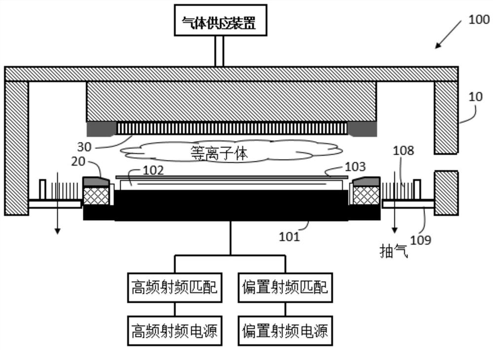
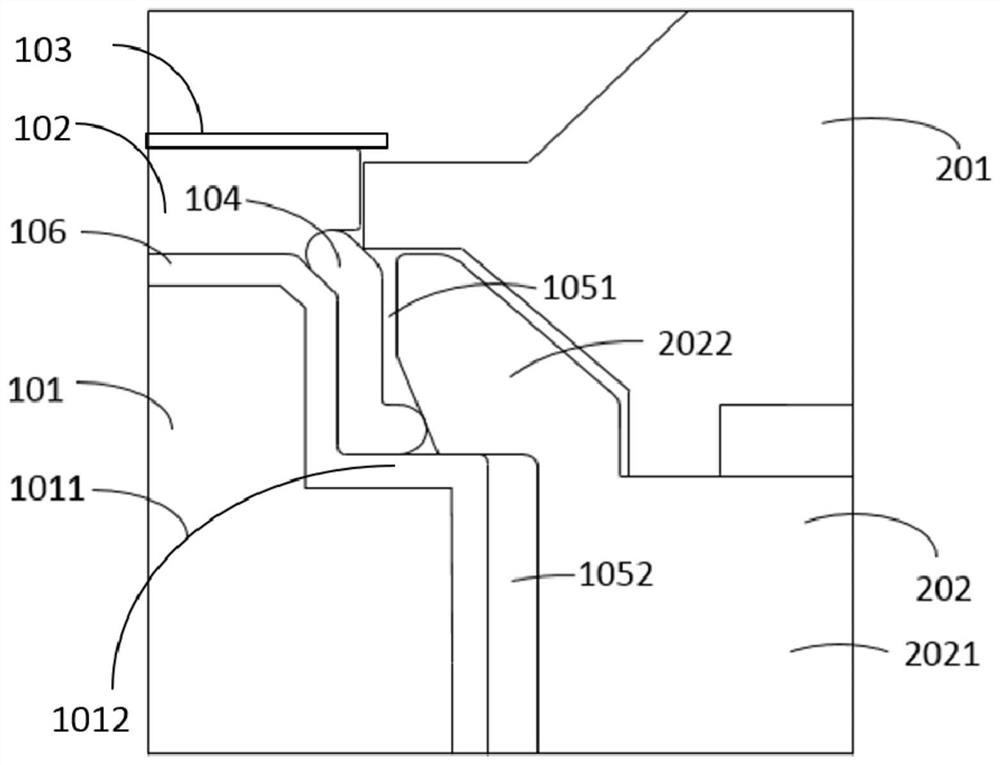
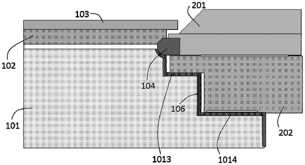
[0037] figure 1 A schematic diagram of a capacitively coupled plasma processing device is shown, including a vacuumable reaction chamber 100 surrounded by an outer wall 10 . The reaction chamber 100 is used for processing the substrate 103 . The interior of the reaction chamber includes a lower electrode assembly, which is used to support t...


PUM


Abstract

According to the lower electrode assembly, the installation method thereof and the plasma processing device, the dielectric ring is matched with the base, the gap between the dielectric ring and the base is divided into two or more gaps, the protection ring is arranged between the dielectric ring and the base, the protection layer is arranged on the outer side of the base, the plasma above the substrate and the focusing ring is prevented from leaking into the gap between the base and the edge ring assembly, the plasma is prevented from corroding the base, the possibility of arc discharge of the lower electrode assembly is reduced, and the use safety of the lower electrode assembly is effectively guaranteed.

Description

technical field [0001] The invention relates to the technical field of plasma etching, in particular to the technical field of plasma processing for preventing arcing of a lower electrode assembly under high radio frequency power. Background technique [0002] Micromachining of semiconductor substrates or substrates is a well-known technique that can be used to fabricate, for example, semiconductors, flat panel displays, light emitting diodes (LEDs), solar cells, and the like. An important step in micromachining manufacturing is the plasma treatment process step, which is carried out inside a reaction chamber into which process gases are fed. A radio frequency source is inductively and / or capacitively coupled to the interior of the reaction chamber to energize the process gas to form and maintain a plasma. Inside the reaction chamber, the exposed substrate is supported by the lower electrode assembly and fixed in a fixed position by a certain clamping force to ensure the sa...

Claims


Application Information

Patent Timeline
IPC IPC(8): H01J37/32H01J9/18
CPCH01J37/32715H01J37/32568H01J9/18
Inventor 赵函一黄国民叶如彬涂乐义
Owner ADVANCED MICRO FAB EQUIP INC CHINA
Why Eureka
Try Eureka