
Circuit board bonding pad correction device

A circuit board, pad technology, applied in the direction of printed circuit repair/correction, printed circuit, printed circuit manufacturing, etc., can solve problems such as waste, pad bending, and circuit board pads that can no longer be used

Active Publication Date: 2021-11-26
怀化海红盛电子科技有限公司
View PDF5 Cites 0 Cited by
  • Summary
  • Abstract
  • Description
  • Claims
  • Application Information

AI Technical Summary

Problems solved by technology

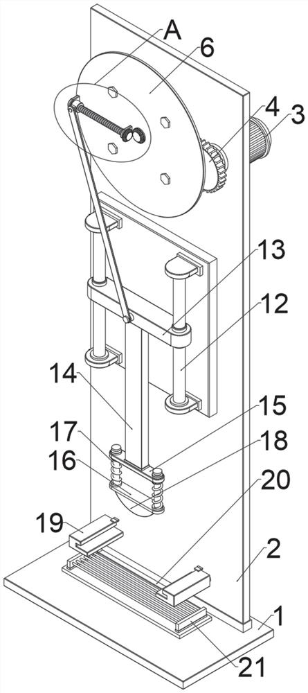
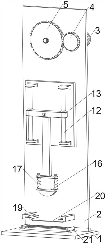
[0005] During the use of circuit board pads, due to temperature or external physical extrusion, it is very easy to cause the pads to bend, and the bent circuit board pads will no longer be used, resulting in a lot of waste. For this reason, we propose a Circuit board pad correction equipment, to realize the correction of the bent circuit board pad

Method used


Image

  • Circuit board bonding pad correction device
  • Circuit board bonding pad correction device
  • Circuit board bonding pad correction device

Examples


Embodiment Construction

[0034] The following will clearly and completely describe the technical solutions in the embodiments of the present invention with reference to the accompanying drawings in the embodiments of the present invention. Obviously, the described embodiments are only some, not all, embodiments of the present invention. Based on the embodiments of the present invention, all other embodiments obtained by persons of ordinary skill in the art without making creative efforts belong to the protection scope of the present invention.

[0035] In addition, an element in the present invention is said to be "fixed" or "disposed on" another element, and it may be directly on another element or an intervening element may also exist. When an element is referred to as being "connected to" another element, it can be directly connected to the other element or intervening elements may also be present. The terms "vertical," "horizontal," "left," "right," and similar expressions are used herein for purp...


PUM


Abstract

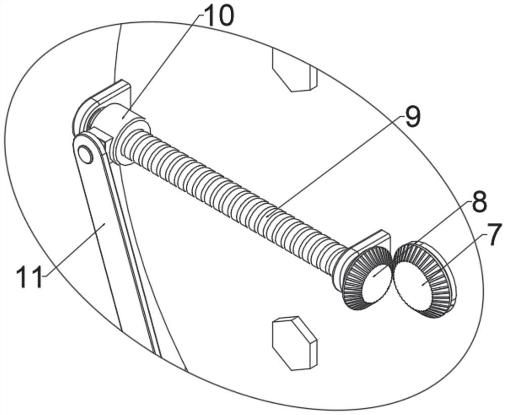
The invention relates to a circuit board bonding pad correction device, and the device comprises a frame structure which is movably provided with a liftable elastic plate, and the elastic plate being used for correcting a bent circuit board bonding pad; a fixing assembly, arranged on the frame body structure and used for carrying a circuit board bonding pad; a tending mechanism, arranged on the frame body structure, and the tending mechanism being used for driving the elastic plate to do lifting motion in the space vertical direction so as to correct a circuit board bonding pad arranged on the fixing assembly, and in the continuous action process of the tending mechanism, the amplitude of driving the elastic plate to do lifting motion being smaller and smaller; a guiding assembly, arranged on the frame body structure and connected with the trend mechanism and the elastic plate, and when the trend mechanism acts, the guiding assembly driving the elastic plate to do lifting motion, so that the bonding pad of the circuit board is corrected.

Description

technical field [0001] The invention relates to the field of circuit boards, in particular to a circuit board pad correction device. Background technique [0002] According to the number of layers, circuit boards are divided into three major categories: single-panel, double-panel, and multi-layer circuit boards. [0003] It is single panel at first, and on the most basic PCB, parts are concentrated on one side, and wires are concentrated on the other side. Because wires only appear on one side, this PCB is called a single-sided circuit board. Single-sided panels are usually easy to manufacture and low in cost, but the disadvantage is that they cannot be applied to too complicated products. Double-sided panels are an extension of single-sided panels. When single-layer wiring cannot meet the needs of electronic products, double-sided panels must be used. There are copper clad and traces on both sides, and the lines between the two layers can be conducted through via holes t...

Claims


Application Information

Patent Timeline
Patent Type & Authority Applications(China)
IPC IPC(8): H05K3/22H05K3/40
CPCH05K3/225H05K3/4007H05K2203/17
Inventor 胡佳杰
Owner 怀化海红盛电子科技有限公司
Learn More