


Quick Research
Generate reliable direction feasibility study reports for your R&D in just a few steps.

Technical Q&A
Discover and master advanced knowledge NOW. Basics, ideas, possibilities, all at once.

Find Solutions
As an expert in R&D theories, this can generate solutions to your technical problems instantly.

Evaluate Feasibility
Analyze your overall solution with one click, know your potential R&D risks in advance.

Monitor Landscape
Get weekly tech updates, stay abreast of the latest tech innovations and key insights.
Silicon wafer box detection clamping frame
A silicon wafer box and clamping frame technology, which is applied in the directions of electromagnetic measuring device, mechanical solid deformation measurement, electric/magnetic solid deformation measurement, etc., can solve the problem that the silicon wafer box is prone to displacement, etc., so as to improve the detection accuracy and prevent Displacement, the effect of improving the detection accuracy
- Summary
- Abstract
- Description
- Claims
- Application Information
AI Technical Summary
Problems solved by technology
Method used
Image

Examples
Embodiment 1
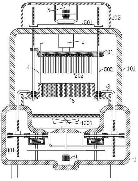
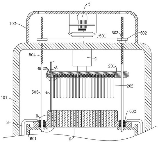
[0027] Embodiment 1: refer to Figure 1-Figure 8 , the silicon wafer box detection clamping frame, including the first box body 1 and the second box body 101, also includes: the first detection plate 202 and the guide rod 505, all can be lifted and connected in the second box body 101; support frame 601, fixedly connected to the top of the first box body 1; the fixed cylinder 602, fixedly connected to the support frame 601, and used to be inserted into the through hole 603 of the wafer box body 6; the fixed cylinder 602 is provided with a guide rod 505 realizes the clamping mechanism for clamping the silicon wafer box body 6; the pressing plate 8 is slidably connected to the first box body 1, and cooperates with the upper surface of the silicon wafer box body 6; A pressing mechanism that controls the downward movement of the pressing plate 8.
[0028] During detection, the wafer box body 6 is placed on the support frame 601, the through hole 603 is sleeved on the fixing cylin...
Embodiment 2
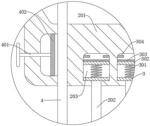
[0040] Embodiment 2: refer to Figure 1-Figure 6 , on the basis of Embodiment 1, further, the pressing mechanism includes a second motor 9 and a second threaded rod 801, the second motor 9 is located in the first box 1, and the second threaded rod 801 is fixedly connected to the pressing plate 8 At the bottom, the second threaded rod 801 is threaded with the second threaded sleeve 1202, the bottom of the second threaded sleeve 1202 is fixedly connected with the sixth gear 1201, and the first rotating shaft 902 and the second rotating shaft 11 are connected in the first box 1 for rotation. The second rotating shaft 11 is fixedly connected with the fifth gear 12 meshed with the sixth gear 1201, the first rotating shaft 902 is provided with a fourth gear 903, and the output end of the second motor 9 is connected with a gear meshed with the fourth gear 903. An automatic slipping mechanism is provided between the third gear 901 , the first rotating shaft 902 and the second rotating...
Embodiment 3
[0048] Embodiment 3: refer to Figure 1-Figure 6 , on the basis of Embodiment 2, further, the output end of the second motor 9 is connected with a ratchet 13 and a fan 1301, and the top of the first box 1 is connected with a protective net 1302, and the ratchet 13 and the fan 1301 are located on the protective net 1302 At the bottom, the top of the first box body 1 is provided with an air outlet 14 , and the bottom of the air outlet 14 is connected with a pipe 1401 .
[0049] The second motor 9 drives the fan 1301 to rotate, forming a negative pressure at the protective net 1302, sucking the dust in the air outlet 14, and the dust around the detection frame is discharged through the pipeline 1401 by the fan 1301, so as to prevent the dust from affecting the detection result.
[0050] Because the fan 1301 is directly below the detection frame, the airflow will not affect the first detection board 202 .
[0051] When the second motor 9 rotates in the opposite direction, the fan...
PUM
 Abstract
Description
Claims
Application Information
 - R&D Engineer
- R&D Manager
- IP Professional
- Industry Leading Data Capabilities
- Powerful AI technology
- Patent DNA Extraction
Browse by: Latest US Patents, China's latest patents, Technical Efficacy Thesaurus, Application Domain, Technology Topic, Popular Technical Reports.
© 2024 PatSnap. All rights reserved.Legal|Privacy policy|Modern Slavery Act Transparency Statement|Sitemap|About US| Contact US: help@patsnap.com