Automatic residual charge discharge circuit of switching power supply and control method thereof
A residual charge, switching power supply technology, used in electrical components, output power conversion devices, irreversible AC power input into DC power output and other directions, can solve the problem of manual discharge of energy storage capacitors, electric shocks, and energy storage capacitors. It is difficult to obtain venting and other issues to achieve the effects of low power consumption, fast response speed and strong venting ability
- Summary
- Abstract
- Description
- Claims
- Application Information
AI Technical Summary
Problems solved by technology
Method used
Image
Examples
Embodiment 1
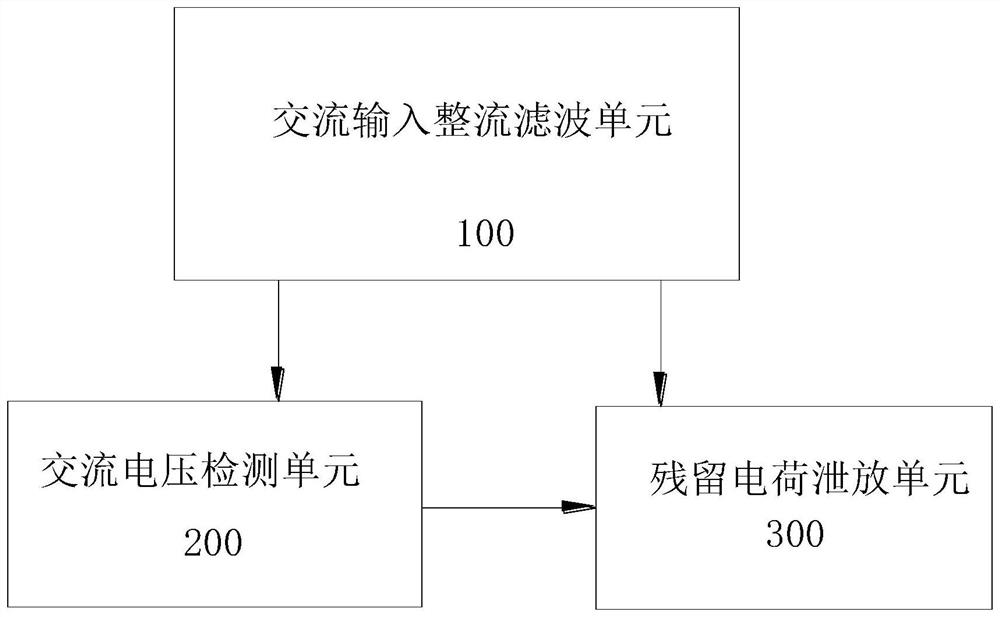
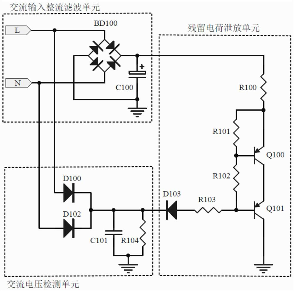
[0028] see figure 1 , in an embodiment of the present invention, a capacitor discharge control circuit includes an AC input rectification and filtering unit 100, a residual charge discharge unit 300, and an AC voltage detection unit 200;
[0029] see again figure 1 , the input end of the input rectification filter unit is connected to the AC voltage, and the output end of the input rectification filter unit is connected to the input end of the residual charge discharge unit 300;
[0030] Thus, it should be noted that the input rectification and filtering unit is used for rectifying and filtering the AC voltage and storing charges in the energy storage capacitor.
[0031] see again figure 1 , the input terminal of the AC voltage detection unit 200 is connected to the input terminal of the AC input filter unit, and the output terminal of the AC voltage detection unit 200 is connected to the control terminal of the residual charge discharge unit 300;
[0032] Thus, it should b...
Embodiment 2
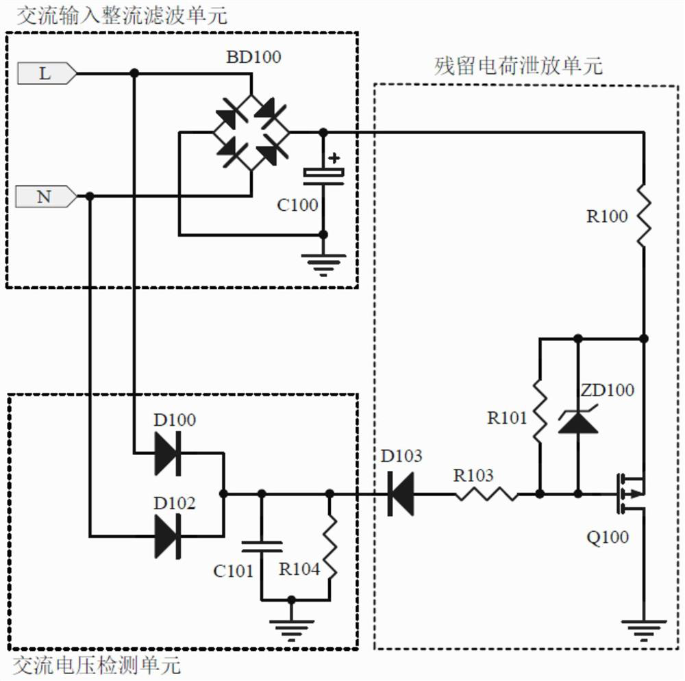
[0046] refer to figure 1 , 3 The difference from Embodiment 1 is that the residual charge discharge unit 300 includes a P-type MOS transistor Q100, three resistors R100, R101, R103, a diode D103, a Zener diode ZD100, and one end of the resistor R100 It is connected to the positive pole of the energy storage capacitor of the AC input rectification filter unit 100, the other end is connected to one end of the resistor R101 and the source of the MOS transistor Q100, the other end of the resistor R101 is connected to the gate of the MOS transistor Q100 and one end of the resistor R103, and the gate of the MOS transistor Q100 One end of the resistor R103 is connected, the other end of the resistor R103 is connected to the anode of the diode D103, the drain of the MOS transistor Q100 is grounded, the anode of the Zener diode ZD100 is connected to the gate of the MOS transistor Q100, and the cathode of the Zener diode ZD100 is connected to the source of the MOS transistor Q100.
[0...
PUM
 Abstract
Description
Claims
Application Information
 - R&D Engineer
- R&D Manager
- IP Professional
- Industry Leading Data Capabilities
- Powerful AI technology
- Patent DNA Extraction
Browse by: Latest US Patents, China's latest patents, Technical Efficacy Thesaurus, Application Domain, Technology Topic, Popular Technical Reports.
© 2024 PatSnap. All rights reserved.Legal|Privacy policy|Modern Slavery Act Transparency Statement|Sitemap|About US| Contact US: help@patsnap.com


