ESD protection device for fully-depleted silicon-on-insulator and preparation method of ESD protection device

A silicon-on-insulator, ESD protection technology, used in semiconductor/solid-state device manufacturing, electrical solid-state devices, semiconductor devices, etc., can solve the problems of difficulty in preparing high-voltage ESD protection devices, narrowing windows, and many chips.

Active Publication Date: 2021-10-29
MICROTERA SEMICON (GUANGZHOU) CO LTD
View PDF7 Cites 2 Cited by
  • Summary
  • Abstract
  • Description
  • Claims
  • Application Information

AI Technical Summary

Problems solved by technology

First of all, the gate dielectric and isolation of small-sized devices are thinner, which leads to the weakening of the device's ability to withstand static electricity, thus narrowing the window for ESD device design
Second, more and more modules are integrated on the same silicon substrate, resulting in more and more risks for chips to suffer from ESD
In addition, silicon-on-insulator (SOI) devices, especially fully depleted silicon-on-insulator (FDSOI) devices, have thin top layers, making it difficult to prepare high-voltage ESD protection devices

Method used


Image

  • ESD protection device for fully-depleted silicon-on-insulator and preparation method of ESD protection device
  • ESD protection device for fully-depleted silicon-on-insulator and preparation method of ESD protection device
  • ESD protection device for fully-depleted silicon-on-insulator and preparation method of ESD protection device

Examples


Embodiment 1

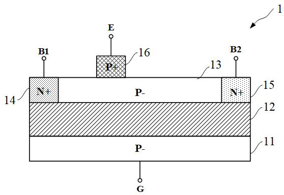
[0044] Such as figure 1 As shown, this embodiment provides a fully depleted silicon-on-insulator ESD protection device 1. The fully depleted silicon-on-insulator ESD protection device 1 includes: a bottom silicon 11, a buried oxide layer 12, a top silicon 13, a first N Type heavily doped region 14, second N type heavily doped region 15, P type heavily doped region 16, first base electrode B1, second base electrode B2, emitter electrode E and gate electrode G.

[0045] Such as figure 1 As shown, the underlying silicon 11 is located at the bottom of the fully depleted silicon-on-insulator ESD protection device 1 .

[0046] Specifically, in this embodiment, the underlying silicon 11 has P-type low doping, the doping ion is boron, and the doping concentration is 10 15 cm -3 ; In actual use, the corresponding doping ions and doping concentration can be selected according to actual needs, not limited to this embodiment.

[0047] Such as figure 1 As shown, the buried oxide layer...

Embodiment 2

[0069] Such as Figure 6~Figure 8 As shown, this embodiment provides a method for manufacturing a fully depleted silicon-on-insulator ESD protection device. As an example, the structure of the fully depleted silicon-on-insulator ESD protection device is the same as that of the first embodiment. The preparation method of the fully depleted silicon-on-insulator ESD protection device comprises:

[0070] S1: Provide a P-type SOI structure, the SOI structure includes a bottom layer of silicon, a buried oxide layer and a top layer of silicon stacked in sequence.

[0071] Specifically, such as Figure 6 As shown, this embodiment is based on the fully depleted silicon-on-insulator process, and firstly an SOI substrate structure is provided, and the SOI substrate structure includes the bottom silicon 11 , the buried oxide layer 12 and the top silicon 13 stacked in sequence. The method for preparing the SOI substrate structure is not limited, and any method that can obtain the SOI sub...


PUM

PropertyMeasurementUnit
thicknessaaaaaaaaaa
thicknessaaaaaaaaaa

Abstract

The invention provides an ESD protection device for a fully-depleted silicon-on-insulator and a preparation method of the ESD protection device. The device comprises bottom layer silicon which has P-type low doping, a buried oxide layer which is formed on the bottom layer silicon, a top layer silicon which is formed on the buried oxide layer and has P-type low doping, a first N-type heavily doped region which is formed in the top layer silicon, a second N-type heavily doped region which is formed in the top layer silicon, a P-type heavily doped region which is formed on the top layer silicon between the first N-type heavily doped region and the second N-type heavily doped region, a first base electrode which is electrically connected with the first N-type heavily doped region, a second base electrode which is electrically connected with the second N-type heavily doped region, an emitter electrode which is electrically connected with the P-type heavily doped region, and a gate electrode which is electrically connected with the bottom layer silicon. According to the ESD protection device, the unijunction transistor is used for forming a voltage stabilization structure, high-voltage ESD protection is achieved, and the ESD protection device is suitable for the fully-depleted silicon-on-insulator.

Description

technical field [0001] The invention relates to the field of integrated circuits, in particular to a fully depleted silicon-on-insulator ESD protection device and a preparation method thereof. Background technique [0002] As microelectronic devices are shrinking in size and integrating functions, electrostatic protection (Electrostatic discharge, ESD) of chips is becoming more and more important. First of all, the gate dielectric and isolation of small-sized devices are thinner, which leads to the weakening of the device's ability to withstand static electricity, thus narrowing the window for ESD device design. Second, more and more modules are integrated on the same silicon substrate, resulting in more and more risks for chips to suffer from ESD. In addition, silicon-on-insulator (SOI) devices, especially fully depleted silicon-on-insulator (FDSOI) devices, have thin top layers, making it difficult to prepare high-voltage ESD protection devices. [0003] Therefore, how t...

Claims


Application Information

Patent Timeline
Patent Type & Authority Applications(China)
IPC IPC(8): H01L27/02H01L27/12H01L21/84
CPCH01L27/0296H01L27/1203H01L21/84
Inventor 刘森关宇轩刘筱伟刘海彬史林森
Owner MICROTERA SEMICON (GUANGZHOU) CO LTD
Why Eureka
Try Eureka