Memory device and method of fabricating the same
A technology for storage elements and storage cells, which is used in semiconductor/solid-state device manufacturing, electrical components, electrical solid-state devices, etc.
- Summary
- Abstract
- Description
- Claims
- Application Information
AI Technical Summary
Problems solved by technology
Method used
Image
Examples
Embodiment Construction
[0080] In order to make the object, technical solution and advantages of the present invention clearer, the present invention will be described in further detail below in conjunction with specific embodiments and with reference to the accompanying drawings.
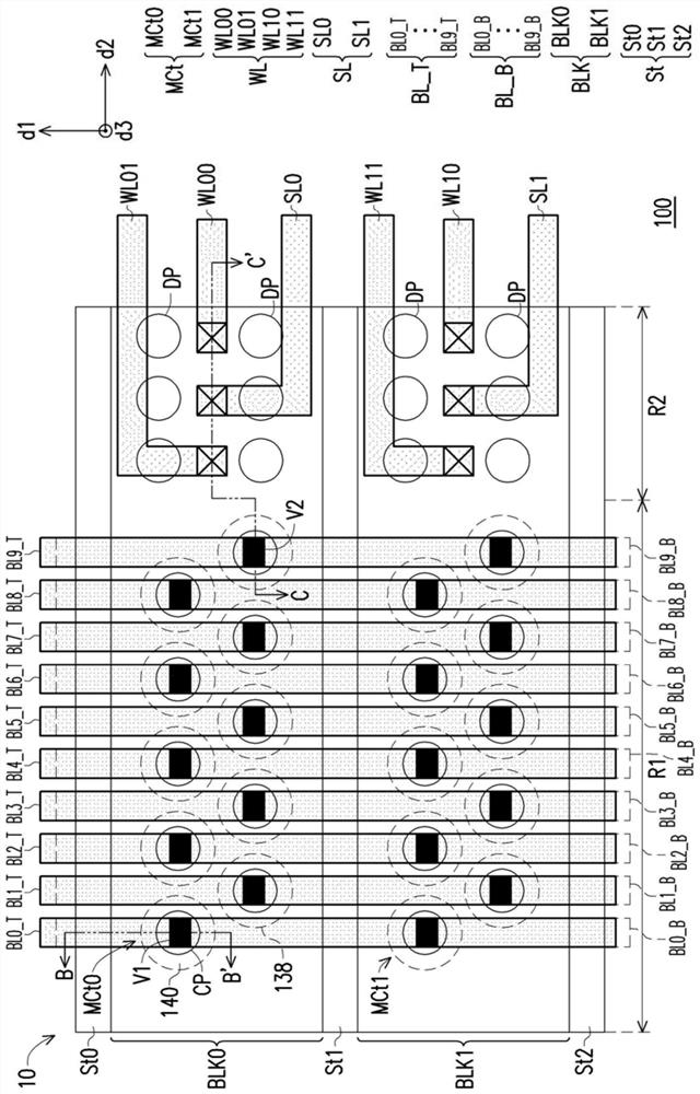
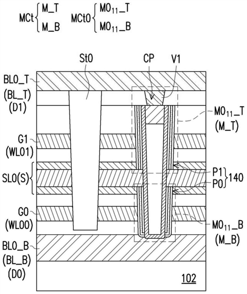
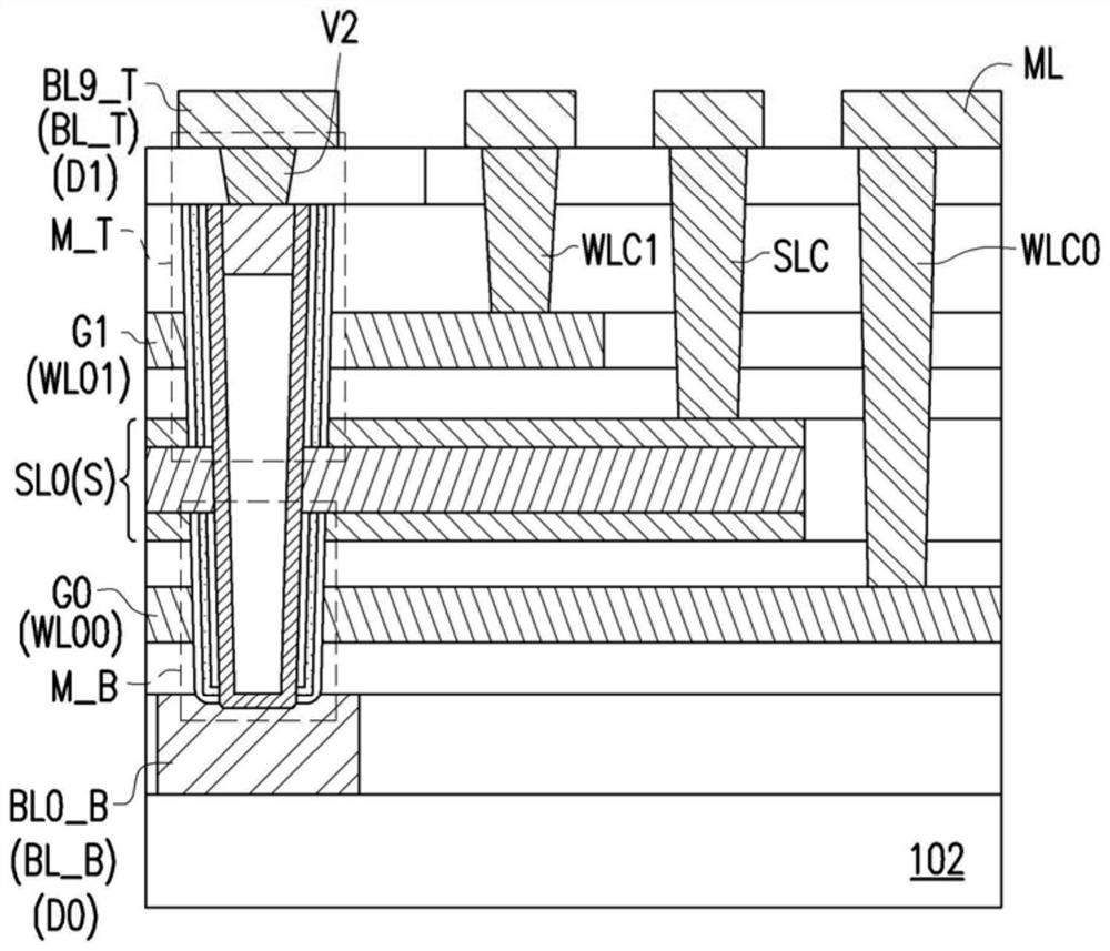
[0081] Please refer to Figure 1A , the memory element 10 of the embodiment of the present invention is a three-dimensional NOR flash memory element, which is disposed on the substrate 100 . The substrate 100 includes a plurality of blocks (Blocks) BLK separated by a plurality of insulation walls St. exist Figure 1A The multiple blocks (Block) BLK are represented by two blocks BLK0 and BLK1, but not limited thereto. The block BLK0 and the block BLK1 are separated by insulation walls (or insulation gaps) St0, St1, and St2. The memory element 10 includes a plurality of memory cell groups MCt located in the first region R1 of each block BLK. The first region R1 may also be called a memory cell region. A plurality of memo...
PUM
 Abstract
Description
Claims
Application Information
 - R&D
- Intellectual Property
- Life Sciences
- Materials
- Tech Scout
- Unparalleled Data Quality
- Higher Quality Content
- 60% Fewer Hallucinations
Browse by: Latest US Patents, China's latest patents, Technical Efficacy Thesaurus, Application Domain, Technology Topic, Popular Technical Reports.
© 2025 PatSnap. All rights reserved.Legal|Privacy policy|Modern Slavery Act Transparency Statement|Sitemap|About US| Contact US: help@patsnap.com


