Electronic component packaging body, electronic component packaging assembly and electronic equipment
A technology of electronic components and packaging components, which is applied in the direction of assembling printed circuits with electrical components, electrical components, printed circuits connected with non-printed electrical components, etc., which can solve the problem of broken solder joints, poor reliability, and affecting the reliability of packaged components and other issues to achieve the effect of improving reliability, ensuring reliability, and reducing the risk of welding failure
- Summary
- Abstract
- Description
- Claims
- Application Information
AI Technical Summary
Problems solved by technology
Method used
Image
Examples
Embodiment 2
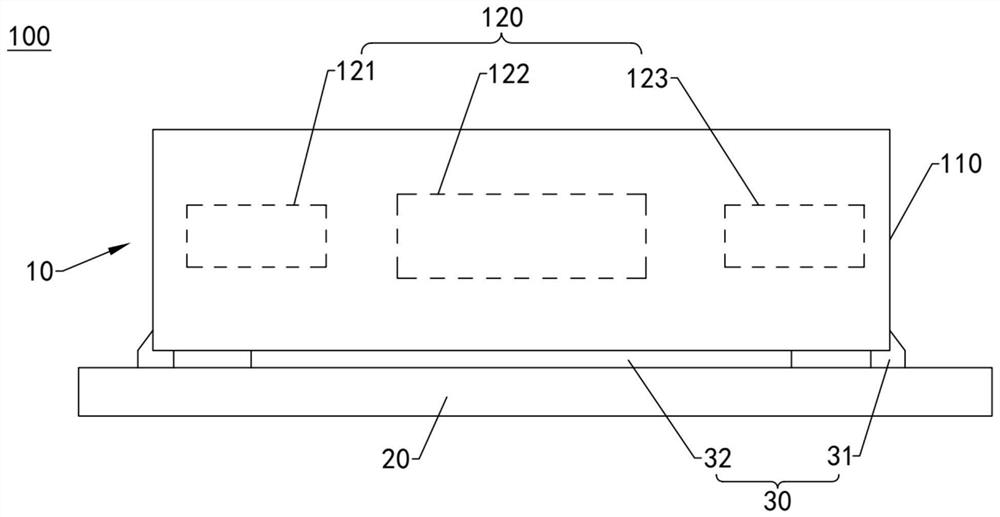
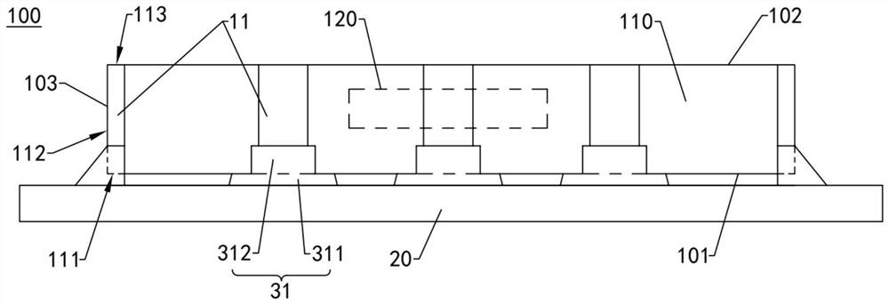
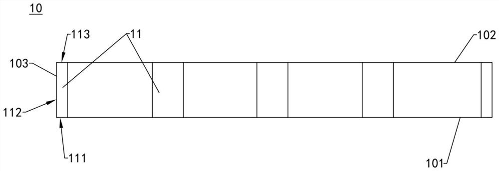
[0117] The difference between the electronic component packaging assembly 100 in the second embodiment and the electronic component packaging assembly 100 in the first embodiment lies in the structure of the electronic component packaging body 10 . understandably, Figure 6a The electronic component package 10 in this application is the second embodiment. For example, the electronic component package 10 includes a substrate 110 , an electronic component 120 packaged inside the substrate 110 , and a first lead 11 electrically connected to the electronic component 120 . At least two adjacently disposed surfaces of the first pins 11 are exposed to the substrate 110 . Exemplarily, the first pin 11 includes a bottom surface 111 of the first pin 11 and a side surface 112 of the first pin 11 connected to the bottom surface 111 of the first pin 11 , and the bottom surface 111 of the first pin 11 faces the circuit board. 20 , and both the bottom surface 111 of the first lead 11 and t...
Embodiment 3
[0127] The difference between the electronic component packaging assembly 100 in the third embodiment and the electronic component packaging assembly 100 in the foregoing embodiments lies in the structure of the electronic component packaging body 10 . understandably, Figure 8 or Figure 9a The electronic component package 10 in this application is the third embodiment. The following mainly describes the differences between this embodiment and the previous embodiments, and most of the same contents of this embodiment and the previous embodiments will not be repeated. For example, the electronic component package 10 includes a substrate 110 , an electronic component 120 packaged inside the substrate 110 , and a first lead 11 electrically connected to the electronic component 120 . At least two adjacently disposed surfaces of the first pins 11 are exposed to the substrate 110 . Exemplarily, the first pin 11 includes a bottom surface 111 of the first pin 11 and a side surface...
Embodiment 4
[0134] The difference between the electronic component packaging assembly 100 in the fourth embodiment and the electronic component packaging assembly 100 in the foregoing embodiments lies in the structure of the electronic component packaging body 10 . understandably, Figure 10 or Figure 11a The electronic component package 10 in this application is the fourth embodiment. The following mainly describes the differences between this embodiment and the third embodiment, and most of the same contents of this embodiment and the third embodiment will not be repeated.
[0135] In this embodiment, the package body 15 is provided with a groove 150 . The components 18 are accommodated in the grooves 150 , and the components 18 are exposed relative to the package body 15 . Figure 10 or Figure 11a The number, shape or position of the middle components 18 are only examples, and are not limited in the present application. Exemplarily, the number of grooves 150 is multiple. A plur...
PUM
 Abstract
Description
Claims
Application Information
 - R&D Engineer
- R&D Manager
- IP Professional
- Industry Leading Data Capabilities
- Powerful AI technology
- Patent DNA Extraction
Browse by: Latest US Patents, China's latest patents, Technical Efficacy Thesaurus, Application Domain, Technology Topic, Popular Technical Reports.
© 2024 PatSnap. All rights reserved.Legal|Privacy policy|Modern Slavery Act Transparency Statement|Sitemap|About US| Contact US: help@patsnap.com


