
Error correction method, error correction device and data refreshing method of memory

An error correction method and memory technology, applied in the field of semiconductor devices and their manufacturing, can solve problems such as unable to recover data correctly, exceeding error correction capabilities, and failing to pass ECC verification

Active Publication Date: 2021-09-10
INST OF MICROELECTRONICS CHINESE ACAD OF SCI
View PDF4 Cites 3 Cited by
  • Summary
  • Abstract
  • Description
  • Claims
  • Application Information

AI Technical Summary

Problems solved by technology

However, ECC also has a certain range of error correction. If the original bit error rate of the read data is high, it will exceed the error correction capability of the error control coding, and the written data cannot be recovered correctly.
[0005]Reference As shown in Figure 1, it is a schematic diagram of a current data storage, the abscissa is the threshold voltage (threshold voltage), and the ordinate is the number of storage cells. In the figure, states E, P1, P2, and P3 are taken as examples for illustration. The solid line represents the initial threshold voltage distribution state formed by the threshold voltage of the memory cell at zero time when data is written into the flash memory, and the dotted line represents the threshold voltage distribution state of the flash memory after a period of storage. It can be seen from the figure that after a period of storage After a period of time, due to the leakage of the charge held by the memory cell, the threshold voltage distribution of the flash memory will shift to the side with a smaller threshold voltage, that is, the distribution will shift to the left. Vread1, Vread2, and Vread3 read the flash memory, which will lead to a high bit error rate of the read data
It is very likely that the ECC check cannot be passed and the correct stored data cannot be obtained

Method used


Image

  • Error correction method, error correction device and data refreshing method of memory
  • Error correction method, error correction device and data refreshing method of memory
  • Error correction method, error correction device and data refreshing method of memory

Examples


Embodiment Construction

[0059] The following will clearly and completely describe the technical solutions in the embodiments of the application with reference to the drawings in the embodiments of the application. Apparently, the described embodiments are only some of the embodiments of the application, not all of them. Based on the embodiments in this application, all other embodiments obtained by persons of ordinary skill in the art without making creative efforts belong to the scope of protection of this application.

[0060] In order to facilitate the understanding of the error correction method of the memory provided by the embodiment of the present application, a specific application scenario of the embodiment of the present application is firstly introduced. A nonvolatile memory includes a plurality of memory cells arranged in an array for storing data. Wherein, the storage unit is divided into several blocks (blocks), and each block is further divided into several pages (pages). Operations su...


PUM


Abstract

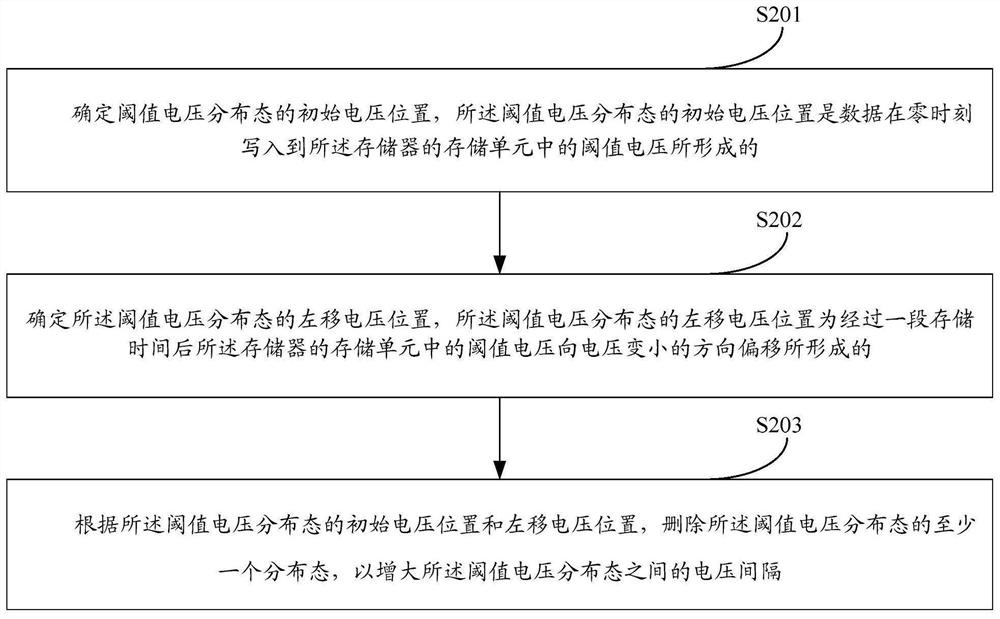
The embodiment of the invention provides an error correction method and device for a memory. The method comprises the steps of: determining initial voltage positions of threshold voltage distribution states, and determining left-shift voltage positions of the threshold voltage distribution states; and deleting at least one distribution state of the threshold voltage distribution states according to the initial voltage positions and the left-shift voltage positions of the threshold voltage distribution states so as to increase the voltage interval between the threshold voltage distribution states. Therefore, in the embodiment of the invention, by determining the initial voltage positions and the left-shift voltage positions of the threshold voltage distribution states, whether data retention error occurs in a memory can be determined; and after data retention error occurs, at least one distribution state of the threshold voltage distribution states is deleted, and the voltage interval between the threshold voltage distribution states is increased, so that the data retention error is reduced, and the data retention time of a storage unit is prolonged.

Description

technical field [0001] The invention relates to the field of semiconductor devices and their manufacture, in particular to an error correction method and device for a memory and a data refresh method for the memory. Background technique [0002] The characteristics of the semiconductor memory device may be volatile or non-volatile, and although the volatile semiconductor memory device can perform read operation and write operation at high speed, the memory stored in the volatile semiconductor memory The content in will be lost. In contrast, nonvolatile semiconductor memory devices are characterized by retaining stored contents regardless of power-on. A flash memory device (Flash memory) is an example of a typical nonvolatile semiconductor memory device, and the flash memory device may be widely used as a data storage medium. [0003] As the demand for large-capacity storage devices increases, multi-level cell memory devices or multi-bit memory devices that store multiple b...

Claims


Application Information

Patent Timeline
IPC IPC(8): G11C29/08G11C29/12G11C29/42
CPCG11C29/08G11C29/12005G11C29/42Y02D10/00
Inventor 王颀杨柳何菁李前辉于晓磊霍宗亮叶甜春
Owner INST OF MICROELECTRONICS CHINESE ACAD OF SCI
Learn More