
Superjunction MOSFET devices and chips

A device and superjunction technology, applied in semiconductor devices, electrical components, circuits, etc., can solve problems such as poor reverse recovery characteristics, and achieve the effect of reducing injection and improving reverse recovery characteristics

Active Publication Date: 2022-04-15
VANGUARD SEMICON CORP
View PDF0 Cites 0 Cited by
  • Summary
  • Abstract
  • Description
  • Claims
  • Application Information

AI Technical Summary

Problems solved by technology

[0003] In view of this, the application provides a super junction MOSFET device and chip to solve the problem of poor reverse recovery characteristics of existing super junction MOSFET devices

Method used


Image

  • Superjunction MOSFET devices and chips
  • Superjunction MOSFET devices and chips
  • Superjunction MOSFET devices and chips

Examples


Embodiment Construction

[0024] The body diode characteristics of super-junction MOSFET devices are worse than those of conventional MOSFETs. The reason is that super-junction MOSFET devices have alternating PN column structures inside, which makes the unbalanced carriers stored in the withstand voltage layer when the body diode is forward conducting. The concentration is higher, and the non-equilibrium carriers are extracted very quickly during the reverse recovery process of the body diode. During the reverse recovery process, the overshoot of current and voltage is very easy to occur, causing damage to the super-junction MOSFET device, resulting in poor reverse recovery characteristics. In order to solve this problem, the present application proposes a super junction MOSFET device, which can improve reverse recovery characteristics.

[0025] The technical solutions in the embodiments of the present application will be clearly and completely described below in conjunction with the accompanying drawi...


PUM


Abstract

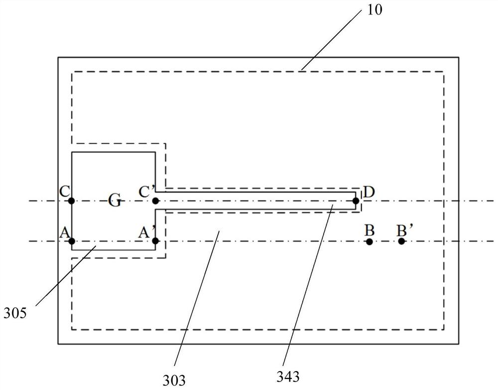
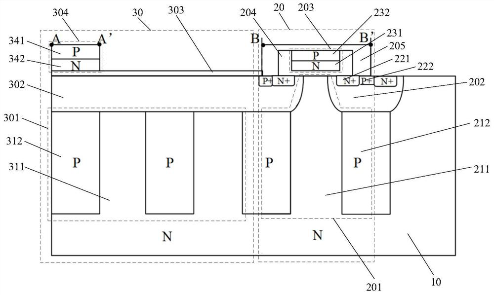
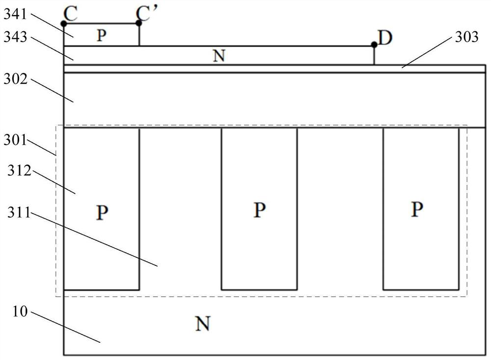
The application discloses a super junction MOSFET device and chip. The super junction MOSFET device includes an N-type epitaxial layer and a cell area and a terminal area located on the N-type epitaxial layer; the cell area includes a first super junction structure, and the upper surfaces on both sides of the first super junction structure are respectively provided with first In the P-type base region, a first polysilicon gate is provided on the upper end surface in the middle of the first super junction structure, and a first oxide layer is provided on the lower surface and both sides of the first polysilicon gate, and the first oxide layer The source metal is provided on the periphery of the second P-type base region; the terminal region includes a second super-junction structure, the upper surface of the second super-junction structure is provided with a second P-type base region, and the upper surface of the second P-type base region is provided with a second oxide layer, A second polysilicon gate is provided on the second oxide layer; by controlling the states of the first polysilicon gate and the second polysilicon gate, a current can be formed on the surface of the first P-type base region. conductive channel. This application can improve reverse recovery characteristics.

Description

technical field [0001] The present application relates to the field of power semiconductor devices, in particular to a super junction MOSFET device and chip. Background technique [0002] The body diode characteristics of super-junction metal-oxide-semiconductor field-effect transistor (Metal-Oxide-Semiconductor Field-Effect Transistor, MOSFET) devices are worse than those of conventional MOSFETs. The reason is that super-junction MOSFET devices have alternating PN column structures. , so that the concentration of non-equilibrium carriers stored in the withstand voltage layer is higher when the body diode is forward-conducting, and the non-equilibrium carriers are extracted very quickly during the reverse recovery process of the body diode. During the reverse recovery process, the overshoot of current and voltage is very easy to occur, causing damage to the super-junction MOSFET device, resulting in poor reverse recovery characteristics. Contents of the invention [0003]...

Claims


Application Information

Patent Timeline
Patent Type & Authority Patents(China)
IPC IPC(8): H01L29/78H01L29/06
CPCH01L29/7827H01L29/0634H01L29/0684
Inventor 任敏李长泽李泽宏林泳浩李伟聪
Owner VANGUARD SEMICON CORP
Learn More