Optical element and manufacturing method thereof

A technology of optical components and normal direction, applied in optical components, optics, polarizing components, etc., can solve the problem that the lamination accuracy of multi-layer films affects the light transmittance, haze and thickness of optical components, and the manufacturing steps of optical components are complicated , affecting the light path, etc., to improve the stress problem and the flatness of the film, save manufacturing costs, and achieve the best optical performance.

Pending Publication Date: 2021-08-06
INTERFACE TECH CHENGDU CO LTD +3
View PDF9 Cites 0 Cited by
  • Summary
  • Abstract
  • Description
  • Claims
  • Application Information

AI Technical Summary

Problems solved by technology

[0003] However, the existing manufacturing process makes the manufacturing steps of optical elements complicated due to the need to perform a bonding step
In addition, if the multi-layer film is attached at the same time, the polarization effect will be unsatisfactory due to the accumulation of high stress, and the multi-layer film will cause the optical element to thicken
Finally, the lamination accuracy of the multi-layer film will affect the overall light transmittance, haze and thickness of the optical element, and further affect the path of light

Method used


Image

  • Optical element and manufacturing method thereof
  • Optical element and manufacturing method thereof
  • Optical element and manufacturing method thereof

Examples


Embodiment Construction

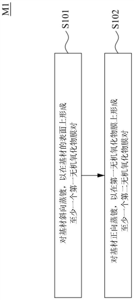
[0040] The following disclosure provides many different embodiments, or examples, for implementing different features of the provided subject matter. Specific examples of components and arrangements are described below to simplify the present disclosure. Of course, these are examples only, and are not intended to be limiting. For example, in the following description a first feature is formed on or on a second feature may include embodiments where the first feature is formed in direct contact with the second feature, and may also include embodiments where additional features may be An embodiment formed between a first feature and a second feature such that the first feature and the second feature may not be in direct contact. In addition, the present disclosure may repeat element symbols and / or letters in various examples. This repetition is for simplicity and clarity and does not in itself indicate a relationship between the various embodiments and / or configurations discuss...


PUM

PropertyMeasurementUnit
transmittivityaaaaaaaaaa

Abstract

A method for manufacturing an optical element comprises the steps that oblique evaporation is conducted on a base material to form at least one first inorganic oxide film pair on the surface of the base material; and forward evaporation is conducted on the base material to form at least one second inorganic oxide film pair on the first inorganic oxide film, and the material of any one of the first inorganic oxide film pair and the second inorganic oxide film pair comprises at least one of a metal element and silicon. By means of the optical element and the manufacturing method of the optical element, the effect of saving the manufacturing cost can be achieved for the optical element with a better optical effect and a smaller film thickness, and a wider application range is achieved.

Description

technical field [0001] The disclosure relates to an optical element and a manufacturing method thereof. Background technique [0002] Nowadays, multi-layer films are often used in the manufacture of optical components to achieve the optical functions of linearly polarized light, circularly polarized light, and semi-transparent and semi-reflected light. For example, a linear polarizer is attached to the optical element, and then an anti-reflection functional film is evaporated on the polarizer by evaporation, so that the optical element can achieve the optical function of polarized light and anti-reflection. [0003] However, the existing process requires a bonding step, which makes the manufacturing steps of the optical element complicated. In addition, if the multi-layer film is attached at the same time, the polarization effect will be unsatisfactory due to the accumulation of high stress, and the multi-layer film will cause the optical element to thicken. Finally, the l...

Claims


Application Information

Patent Timeline
Patent Type & Authority Applications(China)
IPC IPC(8): C23C14/24C23C14/06C23C14/08C23C14/10C23C14/14G02B1/115G02B5/30
CPCC23C14/24C23C14/083C23C14/0694C23C14/0652C23C14/0676C23C14/10C23C14/081C23C14/086C23C14/08C23C14/14G02B5/30G02B1/115
Inventor 施宏欣柯泰年
Owner INTERFACE TECH CHENGDU CO LTD
Why Eureka
Try Eureka