Visual inspection system for upper surface and lower surface of PCB and working method

A PCB circuit board, visual inspection technology, used in measuring devices, optical testing flaws/defects, material analysis by optical means, etc., can solve position and spacing errors, cannot perform double-sided simultaneous inspection, complex flip structure, etc. question

Inactive Publication Date: 2021-07-23
宋志龙
View PDF5 Cites 0 Cited by
  • Summary
  • Abstract
  • Description
  • Claims
  • Application Information

AI Technical Summary

Problems solved by technology

[0002] The internal PCB board of products such as ring-shaped LED lights and wireless chargers has a ring-shaped structure. The ring-shaped bare PCB board is detected by industrial cameras instead of human eyes, and the position and spacing of components on the board are wrong, and the size of lines and components is detected. Errors, wrong component shapes, open sections of lines, contamination on the board, etc.; the existing PCB board can only be tested on one side when testing, and can not be tested on both sides at the same time, or it is necessary to design a complex flip structure.

Method used


Image

  • Visual inspection system for upper surface and lower surface of PCB and working method
  • Visual inspection system for upper surface and lower surface of PCB and working method
  • Visual inspection system for upper surface and lower surface of PCB and working method

Examples


Embodiment Construction

[0050] The present invention will be further described below in conjunction with the accompanying drawings.

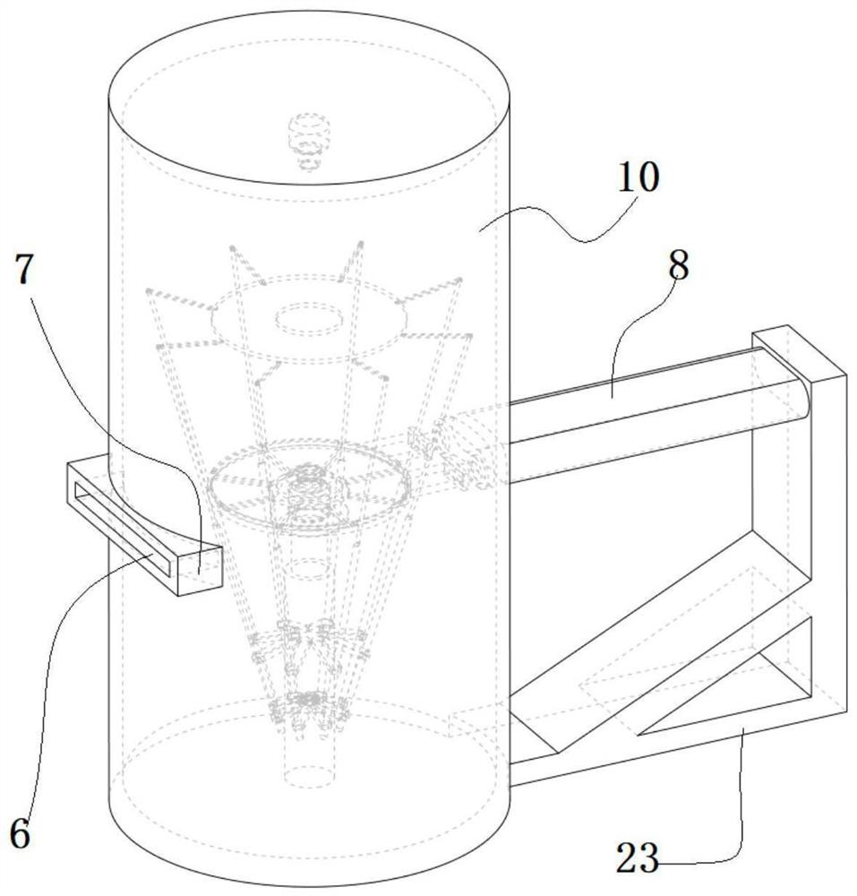
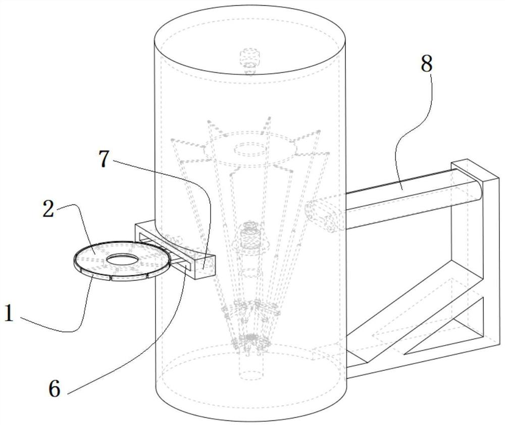
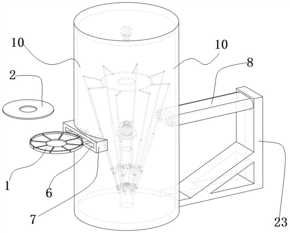
[0051] as attached Figures 1 to 14 The upper and lower visual detection system of the PCB circuit board shown includes a visual detection box body 10, and the visual detection box body 10 is a vertical visual detection darkroom 9, and the middle height of the visual detection darkroom 9 is provided with an overall circular shape. The PCB board placement platform 1, the ring-shaped PCB board 2 to be detected can be horizontally placed on the ring-shaped PCB board placement platform 1; the visual detection darkroom 9 in the present embodiment is provided with a light source for visual detection, and the second used in this program Both the first visual detection camera 32 and the second visual detection camera 11 are CCD cameras.

[0052] One side of the visual inspection box 10 is integrally provided with a mouth seat 7, and the mouth seat 7 is provided with a horizon...


PUM


Abstract

The invention discloses a visual inspection system for the upper surface and lower surface of a PCB. The system comprises a visual detection box body; a vertical visual detection darkroom is arranged in the visual detection box body; a circular PCB placing platform is arranged at the middle height position in the visual detection darkroom; and a to-be-detected annular PCB can be horizontally placed on the annular PCB placing platform. With the visual inspection system of the invention adopted, double-sided detection of the annular PCB can be realized.

Description

technical field [0001] The invention belongs to the field of PCB circuit boards. Background technique [0002] The internal PCB board of products such as ring-shaped LED lights and wireless chargers has a ring structure. The ring-shaped bare PCB is detected by industrial cameras instead of human eyes, and the position and spacing of components on the board are wrong, and the size of lines and components are detected. Errors, wrong component shapes, open sections of lines, contamination on the board, etc.; the existing PCB boards can only be tested on one side when testing, and cannot be tested on both sides at the same time, or it is necessary to design a complex flip structure. . Contents of the invention [0003] Purpose of the invention: In order to overcome the deficiencies in the prior art, the present invention provides a visual inspection system and working method for the upper and lower sides of a PCB circuit board capable of double-sided detection. [0004] Tech...

Claims


Application Information

Patent Timeline
Patent Type & Authority Applications(China)
IPC IPC(8): G01N21/01G01N21/95
CPCG01N21/01G01N21/95
Inventor 宋志龙
Owner 宋志龙
Why Eureka
Try Eureka