A surface-enhanced Raman sensing substrate based on Fano resonance and its preparation method

A surface-enhanced Raman and Fano resonance technology, applied in the optical field, can solve the problems of complex preparation, high cost, difficult application, etc., and achieve the effects of simple preparation, uniform distribution, and easy application.

Active Publication Date: 2022-07-29
UNIV OF ELECTRONICS SCI & TECH OF CHINA
View PDF0 Cites 0 Cited by
  • Summary
  • Abstract
  • Description
  • Claims
  • Application Information

AI Technical Summary

Problems solved by technology

At present, a variety of nanostructures have been designed to achieve Fano resonance, such as non-concentric ring / disk resonators, nanorod-ring structures, heptamer structures, nanodisk matrices, etc.; however, the preparation is too complicated and the cost is high. problem, difficult to apply

Method used


Image

  • A surface-enhanced Raman sensing substrate based on Fano resonance and its preparation method
  • A surface-enhanced Raman sensing substrate based on Fano resonance and its preparation method
  • A surface-enhanced Raman sensing substrate based on Fano resonance and its preparation method

Examples


Embodiment 1

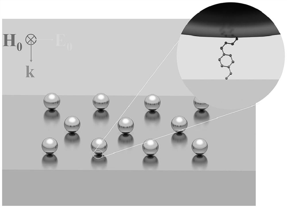
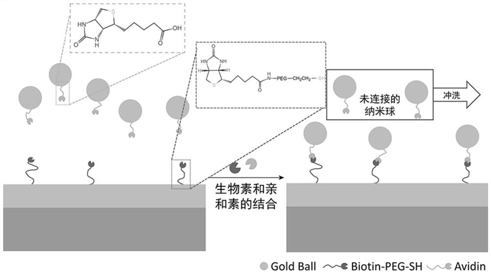
[0042] This embodiment provides a nanosphere-polyethylene glycol-gold film structure surface-enhanced Raman sensing substrate based on Fano resonance, the structure of which is as follows figure 1As shown, the surface-enhanced Raman sensing substrate is prepared on a silicon substrate, and specifically includes: a gold film and nanospheres, wherein the nanospheres are silica nanospheres modified with Avidin (avidin); The surface of the gold film is chemically modified with Biotin-PEG-SH (thiol-polyethylene glycol-biotin) chemical reagent, and the thiol (SH) is strongly chemically linked to the gold film, and PEG (polyethylene glycol) Used to control the length by different molecular weight, Biotin (biotin) and Avidin (avidin) for strong chemical linkage, such as figure 2 and, the surface of the silica nanospheres is covered with a gold-plated layer.

[0043] In this embodiment, in the surface-enhanced Raman sensing substrate structure, the thickness of the gold film is 290nm...

Embodiment 2

[0067] This embodiment provides a nanosphere-polyethylene glycol-gold film structure surface-enhanced Raman sensing substrate based on Fano resonance, the structure of which is as follows figure 1 As shown in the figure, the surface-enhanced Raman sensing substrate is prepared on a silicon substrate, and specifically includes: a gold film and nanospheres, wherein the nanospheres are gold nanospheres, and SH-Avidin (thiol-avidin) is used for the nanospheres. Carry out chemical modification, so that the surface is modified with Avidin (avidin); the surface of the gold film is chemically modified with Biotin-PEG-SH (thiol-polyethylene glycol-biotin) chemical reagent, and the thiol (SH) and the The gold film is strongly chemically linked, PEG (polyethylene glycol) is used to control the length through different molecular weights, and Biotin (biotin) and Avidin (avidin) are strongly chemically linked, such as figure 2 shown.

[0068] Compared with Example 1, the difference betwee...


PUM

PropertyMeasurementUnit
thicknessaaaaaaaaaa
molecular weightaaaaaaaaaa
diameteraaaaaaaaaa

Abstract

The invention belongs to the field of optics, and specifically provides a Fano resonance-based surface-enhanced Raman sensing substrate and a preparation method thereof, which are used to overcome the problems of complicated preparation and high cost of the existing surface-enhanced Raman sensing substrate. In the present invention, the surface-enhanced Raman sensing substrate generates Fano resonance with asymmetric curve characteristics through the resonance coupling of the localized surface plasmon between the nanosphere and the gold film and the mirror imaging field effect; It is chemically connected to the gold film, with strong binding force, stable and not easy to fall off; in addition, the spectral position and intensity of Fano dip can be adjusted by changing the parameters such as the diameter of the nanosphere and the distance between the nanosphere and the gold film. In conclusion, the surface-enhanced Raman sensing substrate provided by the present invention has the advantages of simple preparation, high sensitivity and good uniformity, and can prepare large-scale array structures.

Description

technical field [0001] The invention belongs to the field of optics, relates to surface-enhanced Raman spectroscopy technology, and specifically provides a surface-enhanced Raman sensing substrate based on a Fano resonance nanosphere-polyethylene glycol-gold film structure and a preparation method thereof. Background technique [0002] Surface-enhanced Raman spectroscopy is a technique that is widely used in molecular analysis and characterization. Surface-enhanced Raman has a very complex system; surface-enhanced Raman substrate surface physical structure and surface electronic structure, laser and rough surfaces, and the interaction of surface molecules. Raman spectroscopy is complicated by factors such as interaction, molecular orientation on the surface, bonding interactions, the surrounding environment of the molecule and the surface, the intensity, frequency, polarization, and polarization direction of the incident laser. Generally, surface-enhanced Raman substrates us...

Claims


Application Information

Patent Timeline
Patent Type & Authority Patents(China)
IPC IPC(8): G01N21/65B82Y15/00B82Y40/00
CPCG01N21/658B82Y15/00B82Y40/00
Inventor 龚天巡魏臻江黄文
Owner UNIV OF ELECTRONICS SCI & TECH OF CHINA
Why Eureka
Try Eureka