A microfluidic detection chip structure based on capacitive metamaterial structure artificial surface plasmon and its preparation and detection method
An artificial surface plasmon and detection chip technology, which is applied in the direction of material analysis, material capacitance, and analysis of materials through electromagnetic means, can solve the problems of low resolution and sensitivity, and achieve wide detection range, enhanced consistency, and detection range The effect of high sensitivity
- Summary
- Abstract
- Description
- Claims
- Application Information
AI Technical Summary
Problems solved by technology
Method used
Image


Examples
Embodiment 1
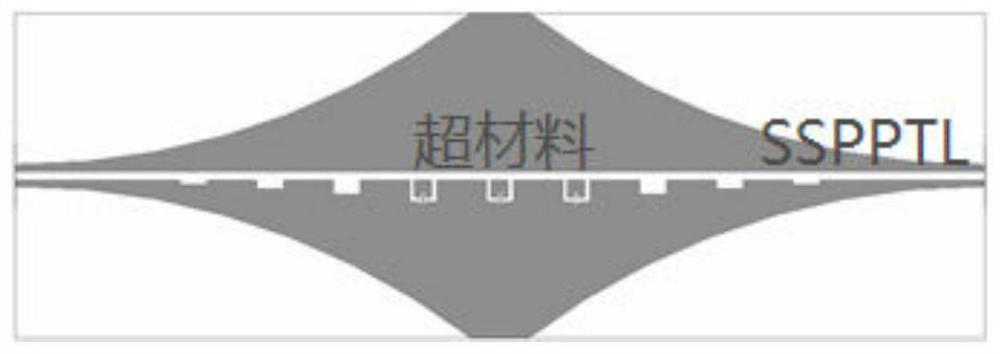
[0057] A microfluidic detection chip structure based on an artificial surface plasmon with a capacitive metamaterial structure, comprising a substrate layer grown sequentially from bottom to top, an artificial surface plasmon metal layer with a capacitive metamaterial structure, Microfluidic channel layer.
[0058] The plane of the substrate layer and the artificial surface plasmonic metal layer with capacitive metamaterial structure is as figure 1 shown. figure 1 SSPPTL is the abbreviation of spoof surface plasmon polaritons transmission line, which means artificial surface plasmon transmission line.
Embodiment 2
[0060] According to the microfluidic detection chip structure of artificial surface plasmon based on capacitive metamaterial structure according to Embodiment 1, the difference is:
[0061] The capacitive metamaterial structure is a split resonant ring structure, a capacitive inductance resonance metamaterial structure, a split ring resonant array structure or a capacitive inductance resonance metamaterial array structure. figure 2 It is a schematic diagram of the split resonant ring structure; image 3 It is a schematic diagram of the structure of the capacitor-inductance resonant metamaterial;
[0062] Figure 4 It is a schematic diagram of the structure of the split resonant ring array; Figure 5 It is a schematic diagram of the structure of the capacitor-inductance resonant metamaterial array;
[0063] Each open resonant ring unit in the artificial plasmonic metal layer with capacitive metamaterial structure is covered by a microfluidic channel in the microfluidic chann...
Embodiment 3
[0067] The preparation method of the microfluidic detection chip structure based on the artificial surface plasmon of the capacitive metamaterial structure described in the embodiment 1 or 2 includes the following steps:
[0068] ①Clean the substrate layer and spin-coat photoresist;
[0069] Cleaning the backing layer, including:
[0070] First, use DECON, deionized water, and acetone to clean the substrate layer in sequence;
[0071] Then, use deionized water to rinse the substrate layer;
[0072] Finally, the substrate layer was blown dry with nitrogen.
[0073] ②Using photolithography technology, define the artificial surface plasmon metal layer pattern with capacitive metamaterial structure on the substrate layer spin-coated with photoresist in step ②, and develop the pattern;
[0074] ③Using electron beam evaporation coating technology and stripping technology, in step ②, the artificial surface plasmon metal layer with capacitive metamaterial structure is evaporated on...
PUM
| Property | Measurement | Unit |
|---|---|---|
| thickness | aaaaa | aaaaa |
Abstract
Description
Claims
Application Information
 - R&D
- Intellectual Property
- Life Sciences
- Materials
- Tech Scout
- Unparalleled Data Quality
- Higher Quality Content
- 60% Fewer Hallucinations
Browse by: Latest US Patents, China's latest patents, Technical Efficacy Thesaurus, Application Domain, Technology Topic, Popular Technical Reports.
© 2025 PatSnap. All rights reserved.Legal|Privacy policy|Modern Slavery Act Transparency Statement|Sitemap|About US| Contact US: help@patsnap.com