Synaptic thin film transistor, preparation method thereof and operation array

A thin film transistor and synaptic technology, applied in the field of microelectronics, can solve the problems of small storage capacity, no jumping out, information processing ability cannot reach the level of human brain intelligence, etc., and achieve the effect of increasing electrical conductivity and improving storage capacity.

Pending Publication Date: 2021-06-25
XIAN JIAOTONG LIVERPOOL UNIV
View PDF4 Cites 0 Cited by
  • Summary
  • Abstract
  • Description
  • Claims
  • Application Information

AI Technical Summary

Problems solved by technology

[0002] Existing computers work according to von Neumann's principles, based on hardware-based information writing and reading, and their structural models and operating mechanisms still do not jump out of the traditional logic operation rules. Therefore, in learning cognition, memory association, The information processing ability of reasoning judgment and comprehensive decision-making is still far from the intelligence level of the human brain. Based on this fact, people have proposed an efficient neuromorphic computing system, which relies on the adjustment of electrical conductivity to realize the change of synaptic weight. Implementing this neuromorphic computing system using synaptic thin-film transistors
In the prior art, the synaptic thin film transistor can only realize two states of on and off, resulting in a small storage capacity when it is used as a storage device, which greatly limits the application of the synaptic thin film transistor in memory chips

Method used


Image

  • Synaptic thin film transistor, preparation method thereof and operation array
  • Synaptic thin film transistor, preparation method thereof and operation array
  • Synaptic thin film transistor, preparation method thereof and operation array

Examples


Embodiment Construction

[0037] The present invention is further detailed in conjunction with the accompanying drawings and examples. It will be appreciated that the specific embodiments described herein are merely illustrative of the invention and are not limited thereto. It will also be noted that in order to facilitate the description, only the parts associated with the present invention are shown in the drawings rather than all structures.

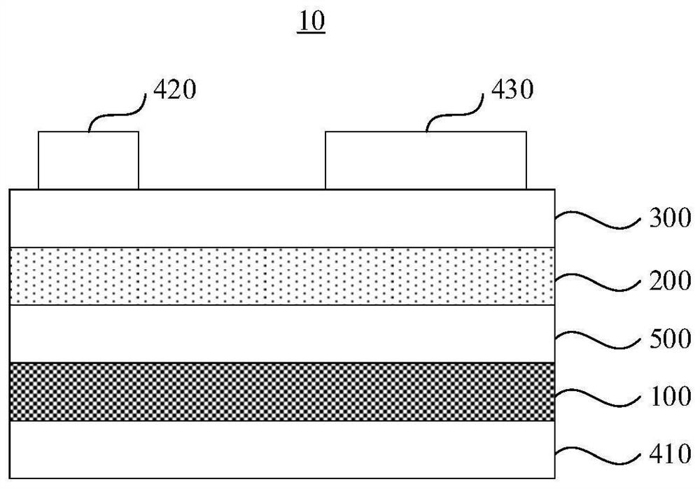
[0038] figure 1 It is a block diagram of a synaptic-type thin film transistor according to an embodiment of the present invention. Such as figure 1 As shown, the synaptic thin film transistor 10 includes a substrate 100; a capture layer 200, a capture layer 200 is disposed on one side of the substrate 100; tunneling layer 300, the tunneling layer 300 is disposed at the capture layer 200 away from the substrate 100 On one side; gate 410, gate 410 is disposed on one side away from the capture layer 200; source 420 and drain 430, source 420 and drain 430 are dispose...


PUM

PropertyMeasurementUnit
thicknessaaaaaaaaaa
thicknessaaaaaaaaaa
thicknessaaaaaaaaaa

Abstract

The invention discloses a synaptic thin film transistor, a preparation method thereof and an operation array. The synaptic thin film transistor comprises a substrate, a capture layer arranged on one side of the substrate, a tunneling layer arranged on one side, far away from the substrate, of the capture layer, a grid electrode arranged on one side, far away from the capture layer, of the substrate, a source electrode and a drain electrode, wherein the source electrode and the drain electrode are arranged on one side, far away from the capture layer, of the tunneling layer, the source electrode and the drain electrode are electrically connected through the tunneling layer, the capture layer is used for providing carriers for the tunneling layer when a preset voltage is applied to the grid electrode. According to the synaptic thin film transistor, the preparation method thereof and the operation array provided by the technical schemes provided by the invention, the electrical conductivity of the synaptic thin film transistor can be accurately adjusted by controlling the voltage applied to the grid electrode of the synaptic thin film transistor, so that a multi-stage storage unit can be realized, and the storage capacity of the operation array is greatly improved.

Description

Technical field [0001] The present invention relates to the field of microelectronics, and more particularly to a synaptic thin film transistor and a preparation method thereof, an array of arranging arranging. Background technique [0002] The existing computer is working in accordance with Von Norman principle, hardware-based information written and reading, and its structural mode and operation mechanism still does not jump out of the traditional logical computing rules, so learning cognition, memory association, The information processing capacity of reasoning judgment, comprehensive decision-making is far from achieving the intelligence level of the human brain, based on this fact, people put forward an efficient neurological computing system, relying on adjustment of conductivity to achieve synaptic weight changes, This neurological calculation system is achieved by a synaptic thin film transistor. In the prior art, the synaptic thin film transistor can only be opened and t...

Claims


Application Information

Patent Timeline
Patent Type & Authority Applications(China)
IPC IPC(8): H01L29/788H01L29/786H01L21/336
CPCH01L29/788H01L29/66825H01L29/66742H01L29/786
Inventor 王琦男赵春赵策洲刘伊娜杨莉
Owner XIAN JIAOTONG LIVERPOOL UNIV
Why Eureka
Try Eureka