Nanometer semiconductor photocatalysis device for air purification

A nano-semiconductor, air purification technology, applied in gas treatment, chemical instruments and methods, membrane technology, etc., can solve the problems of difficult to control catalytic environmental conditions, large volume and difficult to meet market use, etc., to achieve the effect of quiet purification process

Pending Publication Date: 2021-06-01
NANYANG NORMAL UNIV
View PDF17 Cites 0 Cited by
  • Summary
  • Abstract
  • Description
  • Claims
  • Application Information

AI Technical Summary

Problems solved by technology

[0006] In view of the above situation, in order to overcome the defects of the prior art, the present invention firstly provides a nano-semiconductor photocatalytic device for air purification, to solve the problem that the catalytic environmental conditions of the traditional photocatalytic device are difficult to control, and the volume is too large to meet the market requirements.

Method used


Image

  • Nanometer semiconductor photocatalysis device for air purification
  • Nanometer semiconductor photocatalysis device for air purification
  • Nanometer semiconductor photocatalysis device for air purification

Examples


Embodiment Construction

[0024] The specific implementation will be described in further detail below in conjunction with the accompanying drawings.

[0025] The technical solutions in the embodiments of the present invention will be clearly and completely described below in conjunction with the accompanying drawings in the embodiments of the present invention. Obviously, the described embodiments are only some, not all, embodiments of the present invention. Based on the embodiments of the present invention, all other embodiments obtained by persons of ordinary skill in the art without making creative efforts belong to the protection scope of the present invention.

[0026] Those of ordinary skill in the art will recognize that orientation terms such as "upper", "lower", "outer", and "inner" are descriptive terms for the drawings, and do not indicate the scope of protection defined by the claims. limits.

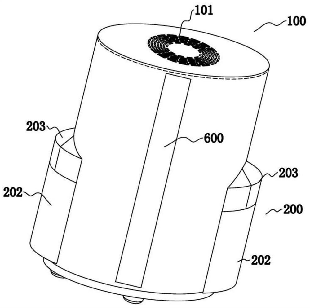
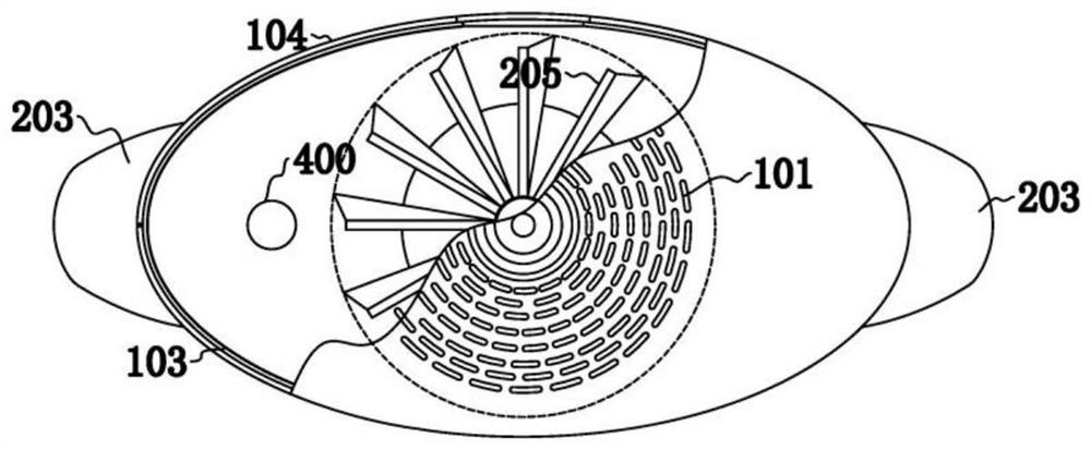
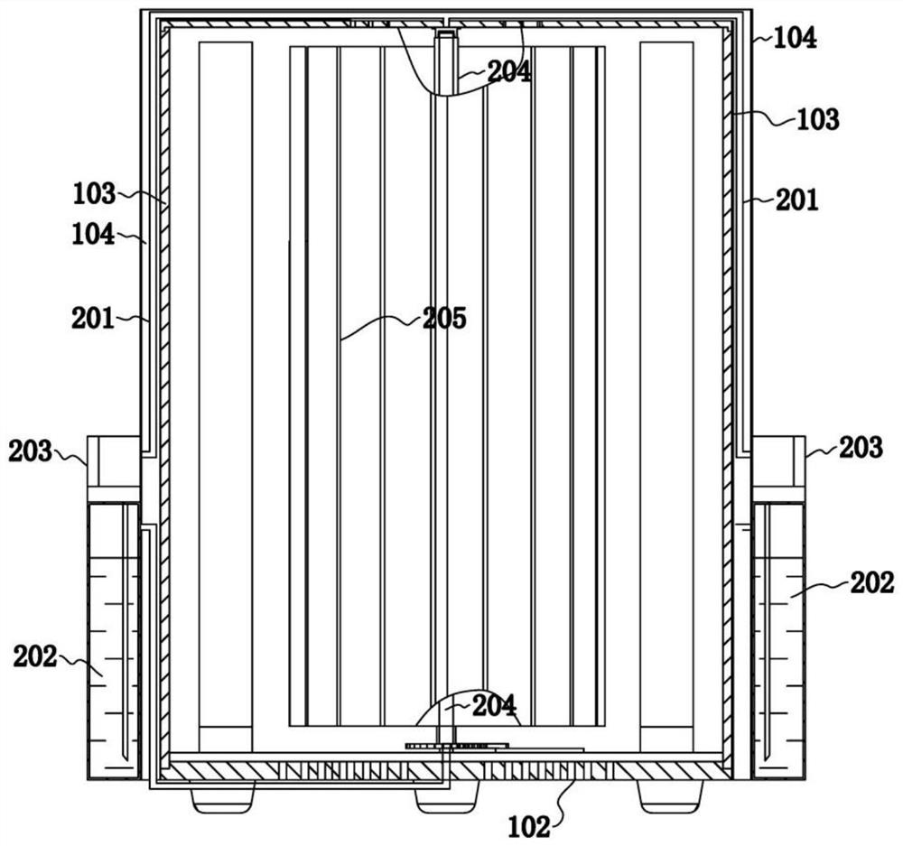
[0027] The housing 100 is provided with an outlet 101 for purified gas at the upper end of the ...


PUM


Abstract

The invention firstly provides a nano semiconductor photocatalysis device for air purification, and aims to solve the problems that a traditional photocatalysis device is difficult in catalytic environment condition control and large in size and is difficult to meet market use. The nano semiconductor photocatalysis device comprises a plurality of membrane-shaped porous metal plates, which are assembled to form an area where the porous metal plates are concentrated, wherein each porous metal plate is provided with three-dimensional communicated pores, the pores are configured to deposit metatitanic acid through a chemical precipitation method, and a titanium dioxide particle layer attached to the surfaces of the porous metal plates is formed through calcination. According to the scheme, the air purification function is achieved through the photocatalytic property of the nanometer semiconductor, the air purification effect is achieved through air exchange and condensate water mist in the cold and hot area exchange process in the purification process, a convection fan does not need to be adopted for driving in the purification process, rich hydroxyl groups can be formed through condensate water, and the device can directly adopt a UV light source for catalysis.

Description

technical field [0001] The invention relates to a photocatalytic device, in particular to a nanometer semiconductor photocatalytic device for air purification. Background technique [0002] Nano-semiconductor materials have a good photocatalytic effect, also known as photocatalyst technology. Specifically, the nanoparticles attached to the effective medium are irradiated by a specific light source, and react with the surrounding water and oxygen in the air to produce extremely strong oxidation. Realize the photolysis and elimination of organic pollutants and some inorganic pollutants in air or water at room temperature, and directly decompose them into harmless and tasteless substances, and can destroy the cell wall of bacteria and kill bacteria, so as to achieve the purpose of treating sewage and waste gas technology for processing and sterilization purposes. [0003] TiO 2 It is an N-type semiconductor material, and its energy band structure is discontinuous. Usually, i...

Claims


Application Information

Patent Timeline
IPC IPC(8): B01D53/86B01D53/44B01D53/38B01D53/26
CPCB01D53/8687B01D53/8678B01D53/007B01D53/265B01D2255/20707B01D2255/802B01D2258/06B01D2259/804
Inventor 王爱华程艺苑赵庆怀盛智铭姬晓旭
Owner NANYANG NORMAL UNIV
Why Eureka
Try Eureka