A mems probe structure for chip testing in ultra-high temperature working environment

A working environment and chip testing technology, applied in the field of MEMS probe structure, can solve the problems that the bare core test work cannot be completed, cannot be guaranteed, and the probe card is damaged

Active Publication Date: 2022-07-05
MAXONE SEMICON CO LTD
View PDF14 Cites 0 Cited by
  • Summary
  • Abstract
  • Description
  • Claims
  • Application Information

AI Technical Summary

Problems solved by technology

[0006] This kind of probe card with guide plate combination structure can realize the bare core test work under most working conditions, however, there are still some bare core test tasks that cannot be completed for the following reasons: In order to make the test real and effective, we need to ensure that the bare core The test environment is consistent with the working environment of the chip. Different chips have different working temperatures. Some chips work in a high temperature environment of about 100 degrees Celsius, while some chips work in an ultra-high temperature environment of 200 degrees Celsius.
For those chips that work in an ultra-high temperature environment, we also need to complete the test in the same temperature environment. Due to the limitation of the probe material, the probe will lose its elasticity in such an ultra-high temperature environment. If you insist on using structures such as intermediate guides or If the method is used to bend the probe, it will cause the probe to be plastically deformed and unable to rebound, not only cannot complete the test work of the bare core, but also will damage the probe card in severe cases
[0007] It can be seen that referring to the solution provided by the invention patent "Probe Device for Vertical Probe Card", although it can be applied to the testing work of most bare cores, it still cannot ensure large size or Effective contact between die and probe during multi-test point chip testing

Method used


Image

  • A mems probe structure for chip testing in ultra-high temperature working environment
  • A mems probe structure for chip testing in ultra-high temperature working environment
  • A mems probe structure for chip testing in ultra-high temperature working environment

Examples


specific Embodiment approach 1

[0091] The following is a specific embodiment of the MEMS probe structure for chip testing in an ultra-high temperature working environment of the present invention.

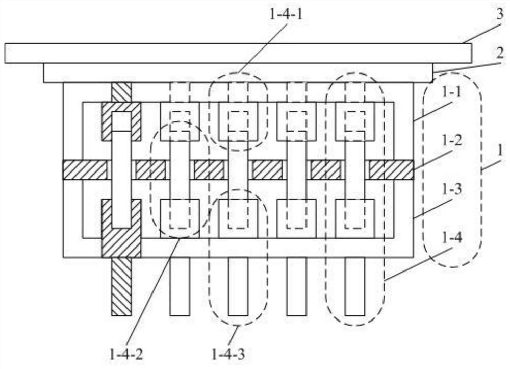
[0092] The structure of the MEMS probe for chip testing under the ultra-high temperature working environment in this embodiment is as follows: figure 1 As shown, the MEMS probe structure is provided with a PCB board 3, an adapter board 2 and a composite probe head structure 1 in sequence from top to bottom. The composite probe head structure 1 includes an upper guide plate 1-1 and a middle guide plate 1-2. and the lower guide plate 1-3, the probes 1-4 start from the adapter plate 2, pass through the upper guide plate 1-1 and the middle guide plate 1-2, and extend from the lower guide plate 1-3; among them, the upper guide plate 1-1 , the middle guide plate 1-2 and the lower guide plate 1-3 are made of insulating material, and the probe 1-4 is made of metal conductive material;

[0093] The probes 1-4 include an...

specific Embodiment approach 2

[0097] The following is a specific embodiment of the MEMS probe structure for chip testing in an ultra-high temperature working environment of the present invention.

[0098] The MEMS probe structure for chip testing in an ultra-high temperature working environment in this embodiment is based on the specific embodiment 1, and further defines that the middle probe 1-4-2 is made of at least one of antimony, bismuth or gallium. Made of metal alloy material. Since antimony, bismuth, and gallium are all substances that expand and contract with heat, they are often used to make alloys to reduce the influence of temperature on precision instruments. Therefore, using them to make the middle probe 1-4-2 can not only meet the electrical conductivity, but also can Realize thermal shrinkage and cold expansion characteristics.

[0099] In addition, the nickel sulfide used to make the tempered glass self-explode is also a substance that expands and contracts with cold, and can also be used...

specific Embodiment approach 3

[0100] The following is a specific embodiment of the chip testing method under the wide temperature range working environment of the present invention.

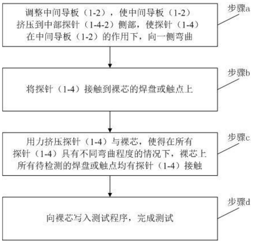
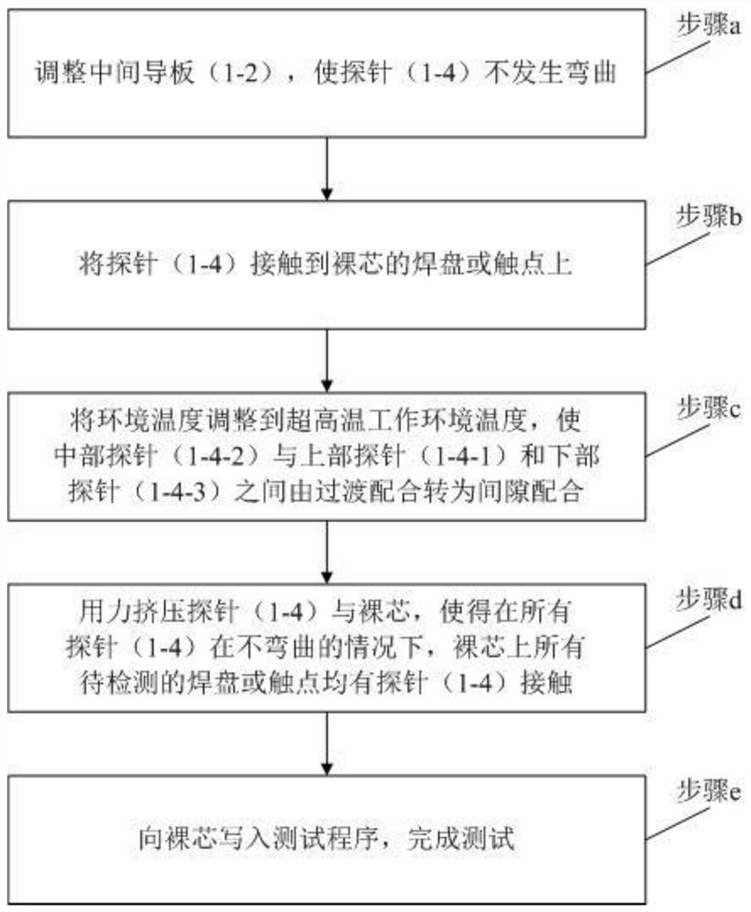
[0101] The chip testing method in the wide temperature range working environment in this embodiment is implemented on the MEMS probe structure for chip testing in the ultra-high temperature working environment described in the specific embodiment 1 or the specific embodiment 2. The wide temperature range working environment The lower chip testing method includes a chip testing method under a conventional temperature working environment and a chip testing method under an ultra-high temperature working environment, wherein the flow chart of the chip testing method under the conventional temperature working environment is as follows figure 2 As shown, the flow chart of the chip testing method in the ultra-high temperature working environment is as follows image 3 shown;

[0102] The normal temperature working environment refe...


PUM


Abstract

The invention relates to a MEMS probe structure for chip testing in an ultra-high temperature working environment, belonging to the technical fields of precision testing and measurement, micro-electromechanical systems, IC chip testing and probe cards; Board and composite probe head structure, the composite probe head structure includes an upper guide plate, a middle guide plate and a lower guide plate. After the probe passes through the upper guide plate and the middle guide plate, it protrudes from the lower guide plate; The needle passes through the middle probe of the middle guide plate and the lower probe installed on the lower guide plate; the upper probe and the lower probe have the characteristics of thermal expansion and cold contraction; the middle probe has the characteristics of thermal contraction and cold expansion; A key technology in the MEMS probe structure and test method for chip testing in the environment is conducive to ensuring effective contact between the bare die and the probe during the testing of large-size or multi-test point chips in an ultra-high temperature working environment, and then It is beneficial to test the chip.

Description

technical field [0001] The invention relates to a MEMS probe structure for chip testing in an ultra-high temperature working environment, belonging to the technical fields of precision testing and measurement, micro-electromechanical systems, IC chip testing and probe cards. Background technique [0002] A probe card is a device used to test bare dies. The performance of the chip is tested by contacting the probes to the pads or contacts of the bare die to form electrical connections, and by writing a test program to the chip. [0003] A key technology to realize the test is that the probes must all be in contact with the pads or contacts of the bare die, which puts forward very high requirements on whether all probe ends are on the same plane. In this application, the extent to which the probe tips are in the same plane is defined as probe flatness. For a probe card with a small size and a small number of probes, the probe flatness is relatively easy to control, while for...

Claims


Application Information

Patent Timeline
Patent Type & Authority Patents(China)
IPC IPC(8): G01R31/28G01R1/073
CPCG01R31/2801G01R1/07328
Inventor 于海超
Owner MAXONE SEMICON CO LTD
Why Eureka
Try Eureka