


Quick Research
Generate reliable direction feasibility study reports for your R&D in just a few steps.

Technical Q&A
Discover and master advanced knowledge NOW. Basics, ideas, possibilities, all at once.

Find Solutions
As an expert in R&D theories, this can generate solutions to your technical problems instantly.

Evaluate Feasibility
Analyze your overall solution with one click, know your potential R&D risks in advance.

Monitor Landscape
Get weekly tech updates, stay abreast of the latest tech innovations and key insights.
Image sensing device
An image sensing and light sensing technology, applied in image communication, TV, color TV components and other directions, can solve problems such as unfavorable signal analysis, voltage value is too small, output signal exceeds dynamic range, etc., to avoid signal value oversized effect
- Summary
- Abstract
- Description
- Claims
- Application Information
AI Technical Summary
Problems solved by technology
Method used
Image

Examples
Embodiment Construction
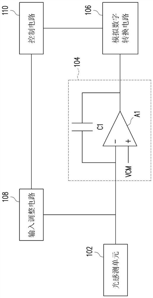
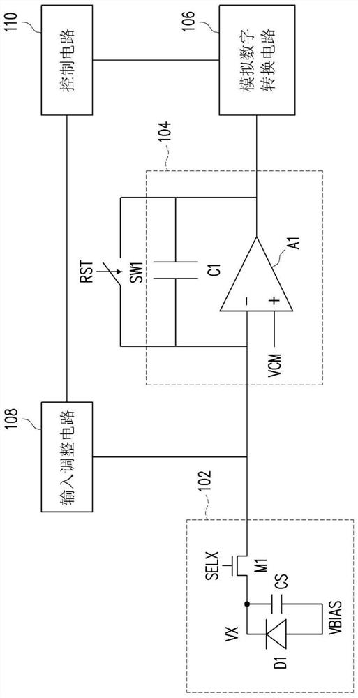
[0015] figure 1 is a schematic diagram of an image sensing device according to an embodiment of the present invention, please refer to figure 1 . The image sensing device may include a light sensing unit 102, an amplifying circuit 104, an analog to digital conversion circuit (Analog to Digital Converter, ADC) 106, an input adjustment circuit 108, and a control circuit 110. The amplifying circuit 104 is coupled to the light sensing unit 102, the analog The digital conversion circuit 106 and the input adjustment circuit 108 , the control circuit 110 is coupled to the analog-to-digital conversion circuit 106 and the input adjustment circuit 108 . In one embodiment, the image sensing device may be, for example, a fingerprint sensor or an X-ray flat panel sensor, but is not limited thereto. Further, the amplifying circuit 104 includes an operational amplifier A1 and a capacitor C1. The negative input terminal of the operational amplifier A1 is coupled to the light sensing unit 10...
PUM
 Abstract
Description
Claims
Application Information
 - R&D Engineer
- R&D Manager
- IP Professional
- Industry Leading Data Capabilities
- Powerful AI technology
- Patent DNA Extraction
Browse by: Latest US Patents, China's latest patents, Technical Efficacy Thesaurus, Application Domain, Technology Topic, Popular Technical Reports.
© 2024 PatSnap. All rights reserved.Legal|Privacy policy|Modern Slavery Act Transparency Statement|Sitemap|About US| Contact US: help@patsnap.com