White-light LED chip packaging structure and manufacturing method thereof

A technology of LED chip and packaging structure, which is applied in the direction of electrical components, circuits, semiconductor devices, etc. It can solve the problems of blue light leakage around the chip, the utilization rate of light has not been effectively improved, and the color of white light is uneven, so as to improve the welding yield. , It is convenient to polish the electrode and avoid the effect of blue light leakage

Inactive Publication Date: 2021-04-06
CHONGQING VOCATIONAL INST OF ENG
View PDF5 Cites 0 Cited by
  • Summary
  • Abstract
  • Description
  • Claims
  • Application Information

AI Technical Summary

Problems solved by technology

[0003] At present, the production of white light LED is mainly made by coating yellow phosphor powder on the blue light chip, that is, directly coating or spraying a layer of phosphor powder on the surface of the blue light LED chip. The white light LED chip produced by the above process is as follows Two problems: one is that only a layer of phosphor glue is coated on the surface of the blue LED chip, but the side of the chip is not coated with phosphor glue, so there will be blue light leakage around the chip, resulting in the white light color of the final packaged white LED device. Uneven, often with yellow or blue spots; Second, the white LED chip prepared by the above method emits light from five sides, and most of the side light becomes ineffective light, and the utilization rate of light has not been effectively improved
In addition, during the production process of the existing white light LED chip, the bottom electrode is easily polluted, which seriously affects the soldering yield of the white light LED chip in the post-process application.

Method used


Image

  • White-light LED chip packaging structure and manufacturing method thereof
  • White-light LED chip packaging structure and manufacturing method thereof
  • White-light LED chip packaging structure and manufacturing method thereof

Examples


Embodiment 1

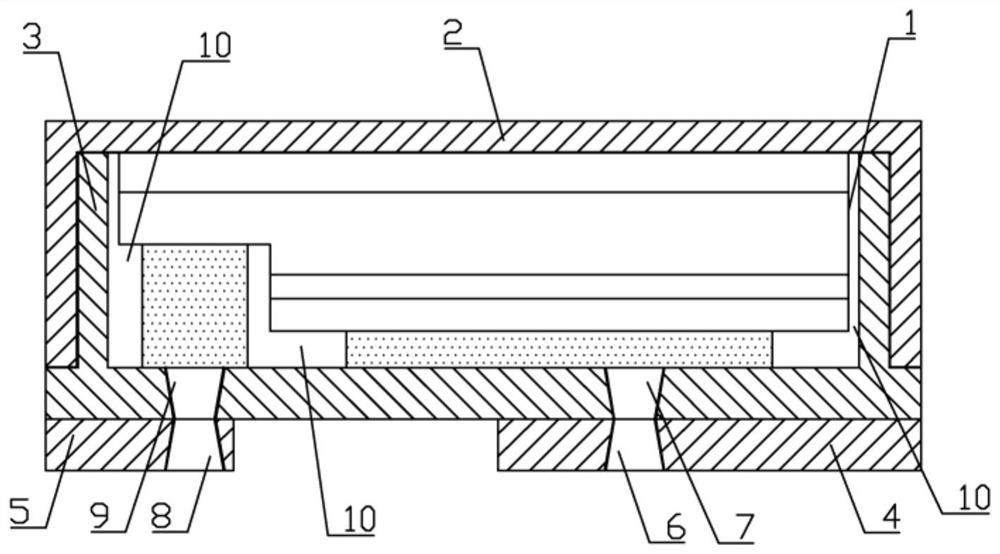
[0033] Such as figure 1 and to figure 2 As shown, a packaging structure of a white LED chip includes a blue LED chip 1, a fluorescent shell 2 for converting light color and a high-reflection white plastic shell 3. The reflective white plastic shell 3 is embedded in the fluorescent shell 2 and forms a closed space with the fluorescent shell 2. The blue LED chip 1 is packaged in the closed space. The LED blue light chip 1 includes a substrate layer 11 and N-type GaN grown on the front surface of the substrate layer 11. Layer 12, the light-emitting layer 13 grown on the front side of the N-type GaN layer 12, the N-type conductive layer 14 grown on the front side of the N-type GaN layer 12, the P-type GaN layer 15 grown on the front side of the light-emitting layer 13, and the P-type GaN layer grown on the front side of the P-type GaN layer. The P-type conductive layer 16 on the front side of the GaN layer 15; the outer bottom surface of the highly reflective white plastic shell...

Embodiment 2

[0041] A method for manufacturing a white light LED chip packaging structure, comprising the following steps:

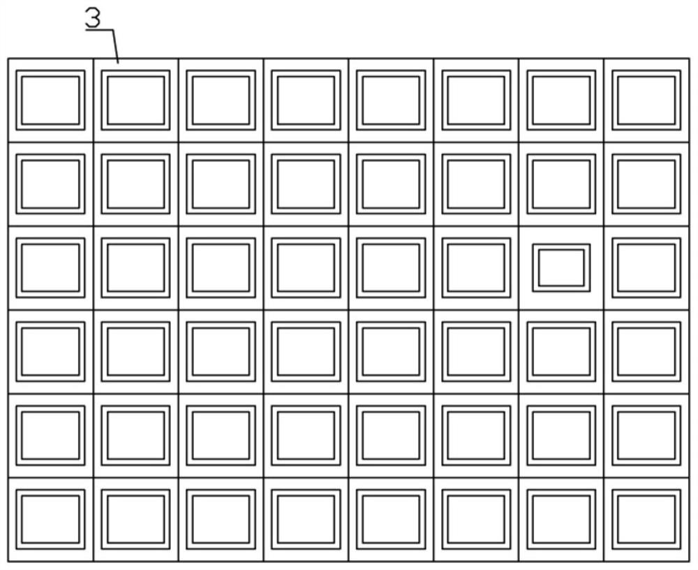
[0042] S1, such as image 3 As shown, make a highly reflective white plastic case 3;

[0043] S2, such as Figure 4 As shown, make a fluorescent shell 2 for converting light color;

[0044] S3, such as Figure 5 As shown, the P-type electrode 4 and the N-type electrode 5 are attached to the outer bottom surface of the high-reflection white plastic shell 3 respectively, and the P-type electrode 4 and the outer bottom surface of the high-reflection white plastic shell 3, the N-type electrode 5 and the high-reflection white plastic shell 3 are made respectively. The through hole on the outer bottom surface of the white plastic shell 3;

[0045] S4, such as Image 6 As shown, the blue LED chip 1 is inverted in the highly reflective white plastic shell 3, and the transparent epoxy resin 10 is filled in the gap between the fluorescent shell 2 and the blue LED chip 1 a...


PUM


Abstract

The invention discloses a white-light LED chip packaging structure and a manufacturing method thereof, belonging to the technical field of semiconductors. The white-light LED chip packaging structure comprises a blue-light LED chip, a fluorescent shell used for converting light colors and a high-reflection white rubber shell, wherein the blue-light LED chip is inversely arranged in the high-reflection white rubber shell; the high-reflection white rubber shell is embedded in the fluorescent shell and forms a closed space with the fluorescent shell; the blue-light LED chip is packaged in the closed space and comprises a substrate layer, an N-type GaN layer growing on the front face of the substrate layer, a light-emitting layer growing on a part of the front face of the N-type GaN layer, an N-type conductive layer growing on a part of the front face of the N-type GaN layer, a P-type GaN layer growing on the front face of the light-emitting layer and a P-type conductive layer growing on a part of the front face. According to the invention, light emitted by the side face of an LED chip can be reflected, effective light output is improved, and the phenomenon of blue light leakage can be avoided; and an electrode can be conveniently ground and even replaced before the welding procedure of LED chip application, so the electrode welding yield of a subsequent procedure can be improved.

Description

technical field [0001] The invention relates to the technical field of semiconductors, in particular to a white light LED chip packaging structure and a manufacturing method thereof. Background technique [0002] Light-emitting diode (LED) is a junction-type electroluminescent semiconductor device that can convert electrical signals into optical signals. Gallium nitride (GaN)-based light-emitting diodes, as solid-state light sources, have been recognized for their high efficiency, long life, energy saving and environmental protection. , small size and other advantages are known as another revolution in the history of human lighting after Edison invented the electric light, and have become the focus of research and development and industry in the international semiconductor and lighting fields. Gallium nitride (GaN), indium gallium nitride (InGaN) , aluminum gallium nitride (AlGaN) and aluminum indium gallium nitride (AlGaInN)-based III-V nitride materials have a continuously...

Claims


Application Information

Patent Timeline
Patent Type & Authority Applications(China)
IPC IPC(8): H01L33/48H01L33/50H01L33/60H01L33/62
CPCH01L33/483H01L33/505H01L33/60H01L33/62H01L2933/0033H01L2933/0041H01L2933/0058H01L2933/0066
Inventor 贺晓辉石磊蒋雨芯赵世纪
Owner CHONGQING VOCATIONAL INST OF ENG
Why Eureka
Try Eureka