Semiconductor cooling and heating composite device and preparation method and application thereof

A composite device and semiconductor technology, which is applied in the manufacture of semiconductor/solid-state devices, semiconductor devices, metal processing equipment, etc., can solve the problems of poor cooling effect, easy loosening of heating wires, and burning of heating wires, etc., to strengthen the fixing effect, improve the Cooling effect, effect of reducing burnout

Pending Publication Date: 2021-02-26
KONFOONG MATERIALS INTERNATIONAL CO LTD
View PDF3 Cites 2 Cited by
  • Summary
  • Abstract
  • Description
  • Claims
  • Application Information

AI Technical Summary

Problems solved by technology

However, transmission between the heating area and the cooling area is required, which cannot achieve a good heating and cooling effect
[0005] CN109355710A discloses a controllable rapid cooling system and method of a semiconductor wafer in a vacuum chamber. The controllable rapid cooling system of a semiconductor wafer in a vacuum chamber can cool the structure to be cooled in the vacuum chamber without affecting the normal operation of the vacuum chamber. Rapid cooling; and the cooling rate can be flexibly adjusted according to needs, but it is not realized that cooling is carried out in the opening connected to the vacuum chamber, the temperature difference between cold and hot is large, and the cooling effect is poor
[0006] Existing heaters generally only have an upper and lower two-layer structure, which is welded by argon arc welding. On the one hand, the welding surface of argon arc welding is prone to air leakage; on the other hand, the heating channel and cooling channel on the product are connected, which affects the cooling effect
Moreover, the heating wire and the heating base plate are not fixed firmly, and the heating wire is easy to loosen during the heating process, resulting in the heating wire being blown and the product being scrapped.
[0007] Therefore, it is necessary to develop a new cooling and heating compound device for semiconductor equipment to overcome problems such as poor cooling effect

Method used


Image

  • Semiconductor cooling and heating composite device and preparation method and application thereof
  • Semiconductor cooling and heating composite device and preparation method and application thereof
  • Semiconductor cooling and heating composite device and preparation method and application thereof

Examples


Embodiment 1

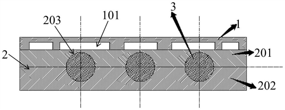
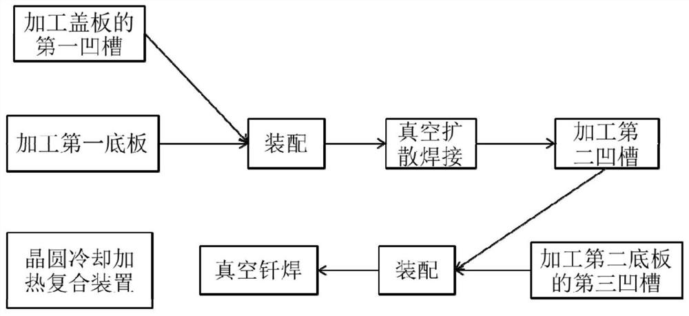
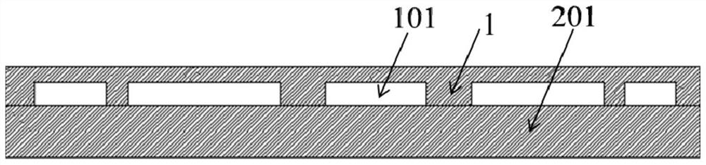
[0079] This embodiment provides a semiconductor cooling and heating composite device, such as figure 1 As shown, the semiconductor cooling and heating composite device includes a cover plate 1 and a bottom plate 2 in turn from top to bottom, the cover plate 1 is provided with at least one first groove 101 opening to the first bottom plate 2012; the bottom plate 2 A slot hole 203 is provided inside, and the slot hole 203 is not in contact with the cover plate 1 , and the slot hole 203 is not in contact with the first groove 101 .

[0080]The bottom plate 2 includes a first bottom plate 2012 and a second bottom plate 2022 sequentially downward from the cover plate 1, and the first bottom plate 2012 is provided with at least one second groove 2031 opening toward the second bottom plate 2022; The bottom plate 2022 is provided with at least one third groove 2032 opening toward the first bottom plate 2012; the second groove 2031 and the third groove 2032 form a circular slot; the se...

Embodiment 2

[0087] This embodiment provides a compound cooling and heating device for semiconductors. The compound cooling and heating device for semiconductors includes a cover plate and a bottom plate sequentially from top to bottom, and at least one first groove opening to the first bottom plate is arranged in the cover plate; A slot is provided inside the bottom plate, and the slot is not in contact with the cover plate, and the slot is not in contact with the first groove.

[0088] The bottom plate includes a first bottom plate and a second bottom plate sequentially from the cover plate downwards, the first bottom plate is provided with at least one second groove opening toward the second bottom plate; At least one third groove of the bottom plate opening; the second groove and the third groove form a circular slot; the second groove is a second semicircular groove; the third groove is a third Semi-circular slot; the radius of the circular slot is 2mm; the flatness of the cover plate...

Embodiment 3

[0095] This embodiment provides a compound cooling and heating device for semiconductors. The compound cooling and heating device for semiconductors includes a cover plate and a bottom plate sequentially from top to bottom, and at least one first groove opening to the first bottom plate is arranged in the cover plate; A slot is provided inside the bottom plate, and the slot is not in contact with the cover plate, and the slot is not in contact with the first groove.

[0096] The bottom plate includes a first bottom plate and a second bottom plate sequentially from the cover plate downwards, the first bottom plate is provided with at least one second groove opening toward the second bottom plate; At least one third groove of the bottom plate opening; the second groove and the third groove form a circular slot; the second groove is a second semicircular groove; the third groove is a third Semi-circular slot; the radius of the circular slot hole is 2.01mm; the flatness of the cov...


PUM

PropertyMeasurementUnit
radiusaaaaaaaaaa
surface smoothnessaaaaaaaaaa
thicknessaaaaaaaaaa

Abstract

The invention discloses a semiconductor cooling and heating composite device and a preparation method and application thereof. According to the semiconductor cooling and heating composite device, a slotted hole is formed in the bottom plate, so that the slotted hole is not connected with the cover plate and the first groove, the isolation of heating in the slotted hole and cooling in the first groove is realized, and the cooling efficiency is greatly improved; according to the preparation method of the semiconductor cooling and heating composite device, vacuum diffusion welding is conducted onthe cover plate and the first bottom plate, no air leakage phenomenon exists after welding, then vacuum brazing is adopted for welding the second bottom plate, fixing of the heating wire can be ensured, the situation that the heating wire is burnt out is reduced, and the semiconductor cooling and heating composite device has wide application prospects in the field of semiconductors.

Description

technical field [0001] The present invention relates to the technical field of semiconductors, in particular to the technical field of semiconductor wafers, in particular to a semiconductor cooling and heating compound device and its preparation method and application. Background technique [0002] In semiconductor wafer heating, it is necessary to use a cooling plate with a heating wire device that can cool the heating wire in real time. At present, argon arc welding or vacuum brazing is generally used to weld the cooling plate. The heating channel communicates with the cooling channel, which affects the cooling effect. [0003] CN105374766A discloses a semiconductor wafer cooling method and a semiconductor wafer cooling device, in which a heated semiconductor wafer is placed on a heated holding table. Cooling is performed while holding the semiconductor wafer so that the semiconductor wafer is spaced above the holding table. In this cooling process, the semiconductor waf...

Claims


Application Information

Patent Timeline
Patent Type & Authority Applications(China)
IPC IPC(8): H01L21/67B23K1/00B23K20/02B23K20/14B23K28/02B23P15/00C22C5/06C22C5/08
CPCB23K1/0008B23K20/023B23K20/14B23K28/02B23P15/00B23K2101/40B23K2103/56C22C5/06C22C5/08H01L21/67098
Inventor 姚力军边逸军潘杰王学泽占卫君廖培君罗明浩
Owner KONFOONG MATERIALS INTERNATIONAL CO LTD
Why Eureka
Try Eureka